3D Xpoint memory doesn’t use transistors and it is made out of some secret material the company didn’t want to talk about. Luckily for us, we had Ken Furnanz, manager of business development non-volatile memory group at EMEA who was willing to answer some questions. According the CEO from Micron, this memory is so cool that people thoughz it is impossible to make.
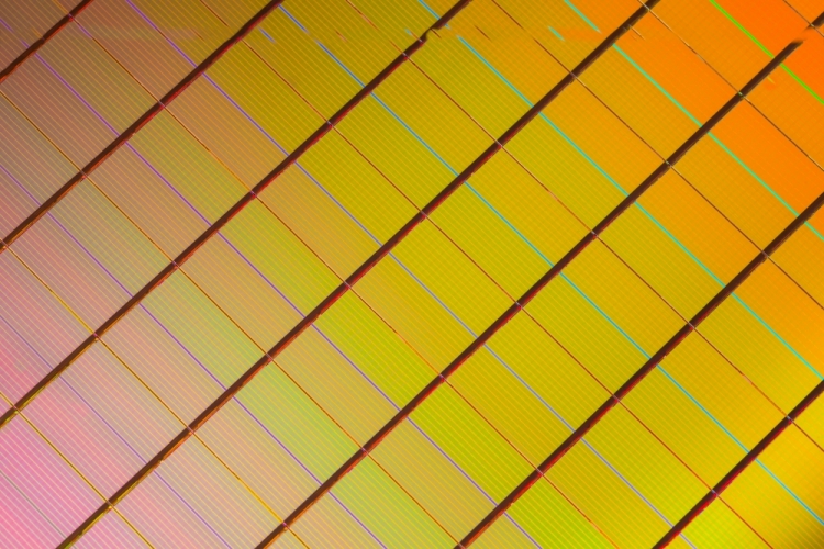
We learned that the 3D Xpoint memory is going to be manufactured in Lehi, Utah, in a IM Flash factory but Ken told us it will be manufactured at 20nm process. Many have assumed that Intel and Micron will use 16nm NAND process but since this is not NAND memory, Intel and Micron chose to do it in 20nm.
With the 20nm manufacturing process they can manufacture 128 Gbit chips (16GB per die) which is on par with Micron MLC 16nm NAND that can provide the same 128Gb MLC device (16GB per die).
The way how it works is the cell that replaces the transistor will change its property and be able to store the data. Clearly this new material can do this really fast.
We also head repeatedly that the products based on 3D Xpoint memory should fill the gap between DRAM devices, that are fast and cannot store data, and NAND devices that are not fast enough, but can store the data once they power down.
We also learned that 20nm manufacturing is just the beginning, and, of course, the memory will eventually will shrink down to 16nm and beyond, and it can also expand adding multiple layers. After all, it is 3D Cross point memory so it can increase its capacity per die in many dimensions.
Ken didn’t want to go into product specifics and just confirmed the samples are shipping this year and products from separately Intel and Micron are expected next year.