This is the first non-volatile memory that sits in a class of its own, and Intel and Micron claim that it is 1,000 times faster than 3D NAND. This means you will have DRAM memory speeds, or slightly slower speeds, on chips that will not forget the data once you turn your device off.
This is the first big innovation in the solid state storage space in 25 years, according to Intel and Micron. The companies have invented unique material compounds and a cross point architecture for a memory technology that is 10 times denser than conventional memory.
Intel Senior Vice President Rob Crooke held a presentation together with Micron CEO Mark Durcan and they both agreed that we need faster memory for storage. Mark said that people believe that is impossible, but apparently this alliance managed to solve this problem.
You need faster memory than today's for massive in-memory databases, fast system recovery, low latency and high endurance. This is what the system administrators around the world have dreamed about for a while. End uses will benefit as well, as it will make loading levels in games faster, enable faster genomics as well as high fidelity pattern recognition.
Micron's boss compared the level of speed and innovation with speed up that we got when we transitioned from mechanical hard drives to NAND based SSDs. In real world applications, we got got a fivefold speed improvement in read and write speeds, jumping from less than 100MB/s read or write to 500 MB/s, so we advise you to take this 1000x faster promise with a huge grain of salt.
Intel warned us that this is a technology announcement and not a product announcement. It deflected all our questions, including what is the base of NAND speed when Intel claims 1000x faster and a few others.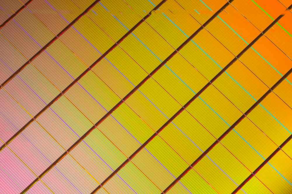
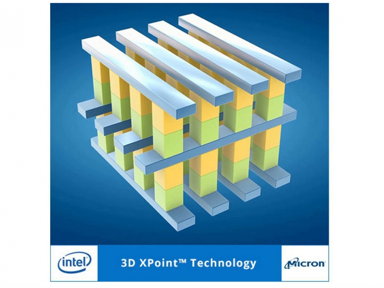
It turns out that the 3D Xpoint technology chips can story 128 Gbits of data (16GB) per chip. This is how the technology roughly works.
Cross Point Array Structure
Perpendicular conductors connect 128 billion densely packed memory cells. Each memory cell stores a single bit of data. This compact structure results in high performance and high density bits.
Selector
Memory cells are accessed and written or read by varying the amount of voltage sent to each selector. This eliminates the need for transistors, increasing capacity while reducing cost.
Fast Switching Cell
With a small cell size, fast switching selector, low-latency cross point array, and fast write algorithm, the cell is able to switch states faster than any existing non-volatile memory technologies today
Stackable
In addition to the tight cross point array structure, memory cells are stacked in multiple layers, much like the levels in a parking garage. The initial technology stores 128Gb per die across two memory layers. Future generations of this technology can increase the number of memory layers, in addition to traditional lithographic pitch scaling, further improving system capacities.
The 3D Xpoint memory is going to be manufactured in Lehi, Utah, in a IM Flash factory. This is a joint venture created by Micron and Intel in 2006. Micron's CEO points up that this is not a Power Point presentation, they already have first wafers and they plan to sample chips later this year. Micron and Intel will separately bring products based on 3D Xpoint memory to the market in 2016.
The best way to see this memory is a device that sits between RAM and NAND – SSD. 3D Xpoint is slower than RAM, but not by much, but it is much faster than a traditional SSD. Make sure you have in mind that these cells are not transistor based, but they can process and store / delete bits and bytes at very high speeds.
3D Xpoint memory is an interesting announcement but it leaves many questions unanswered.