
Index
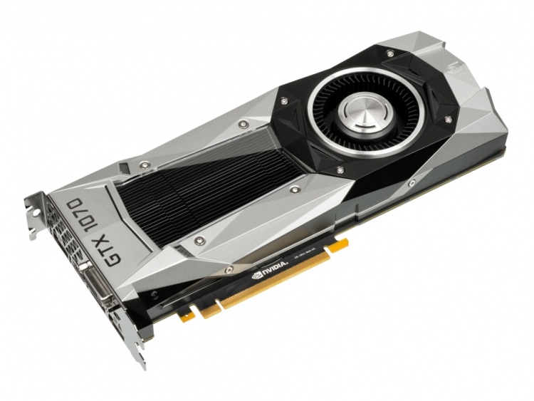
- Nvidia Geforce GTX 1070 Founders Edition review
- Hardware - Inside Nvidia's Founders Edition
- Geforce GTX 1070 Specifications
- Power efficiency and design
- Nvidia's Pascal GP104
- HDR display gaming now supported
- H.264 and HEVC playback on Geforce Pascal
- Single, double and half-precision performance
- PCI-E 3.0 x8 and PCI-E 3.0 x16 bandwidth
- Test setup
- Results - Fallout 4
- Results - Far Cry 4
- Results - No Man's Sky
- Results - The Elder Scrolls V: Skyrim
- Results - Just Cause 3
- Nvidia GPU Boost 3.0
- Conclusion
- All Pages
Nvidia's Pascal GP104
As we mentioned during GTC conference earlier this spring, Nvidia’s full GP100 chip features 15.3 billion transistors in a 610mm^2 die package with 3,584 cores across 56 streaming multiprocessor (SM) clusters containing 64 SMs each.
For the Geforce GTX 1070, the company is using a cut-down version of this die called GP104-200, featuring 7.2 billion transistors in a size estimated at 333m^2. The chip has 1920 cores across 15 SM clusters, 64 ROPs and 120 texture units. Meanwhile, the GP104-400 in the Geforce GTX 1080 has 2560 cores across 20 SM clusters, 64 ROPs and 128 texture units.
It is important to note that Nvidia disabled 5 SM clusters in the Geforce GTX 1070 desktop card and then released the mobile Geforce GTX 1070 variant for notebooks a few weeks ago with 16 SM clusters enabled. The mobile version brings the core count up to 2048 cores with 128 texture units. As some sites point out, however, the benefit of an additional SM cluster is countered by having lower core clock frequencies by about 4 percent over the desktop version. But in terms of peak gigaflops, the notebook Geforce GTX 1070 variant will still deliver 6.74 teraflops at lower frequencies versus 6.46 on desktop.
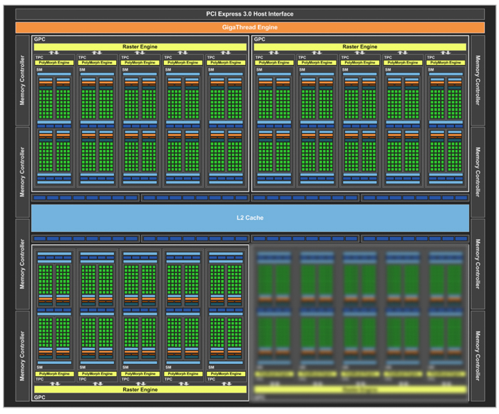
Nvidia GP104-200 block diagram (Larger image here)
In terms of architecture, Pascal shares many similarities with Maxwell in that both cores contain four graphics processing clusters (GPC) each. The GP104-200, however, has one of the four GPCs disabled in the die. When Fermi was introduced several years ago, the company introduced a pipeline unit called the PolyMorph Engine, each of which (16 at the time) contained a vertex fetcher and tessellator, among other key units. All the way up until Maxwell, this unit was integrated into the SMs, but with Pascal it has been reintroduced into a separate Texture Processing Cluster (TPC) that sits between the Raster Engine and each SM block.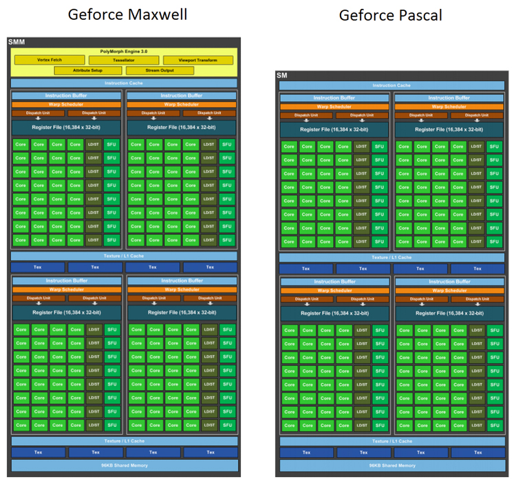
According to some reports, the number of units, engines and ROPs between Maxwell GM204 and Pascal GP104, along with their throughput per-clock speeds make the architectures to be performance identical, at least on paper. The differences can likely be attributed to SM block layout changes, pipeline scheduling patterns, and any new load balancing techniques.
Nvidia is shipping the GTX 1070 with GDDR5 memory while the GTX 1080 receives GDDR5X, and the GP104 features a memory controller with 256-bit width designed to support the tighter signaling demands of GDDR5X while offering backward compatibility with GDDR5. The GTX 1070 operates at 8Gbps frequency and delivers 256GB/s memory bandwidth, while the GTX 1080 operates at 10Gbps frequency and delivers 320MB/s of bandwidth.