Index
- Nvidia GTX 980 reviewed
- The GM204 GPU
- VXGI, dynamic global illumination technique
- MFAA, multi-frame sampled anti-aliasing
- DSR, dynamic super resolution
- A closer look at GTX 980
- Testbed
- 3DMark
- Sleeping Dogs
- Crysis 3
- Thief
- Battlefield 4
- BioShock
- Tomb Raider
- Far Cry 3
- Unigine Heaven
- Thermals and Noise
- Power Consumption
- Conclusion
- All Pages
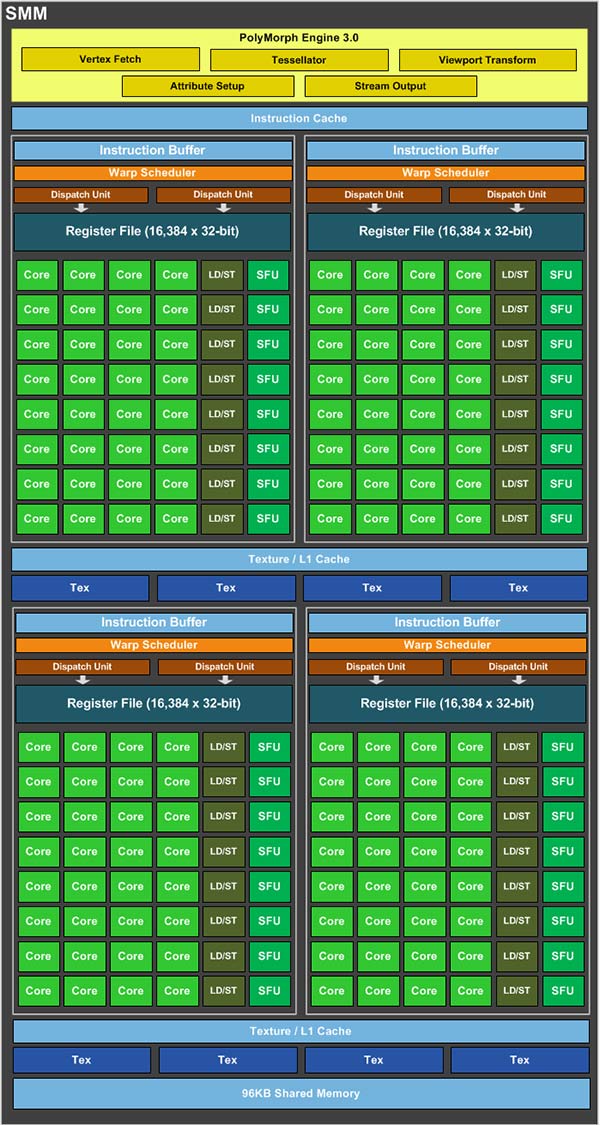
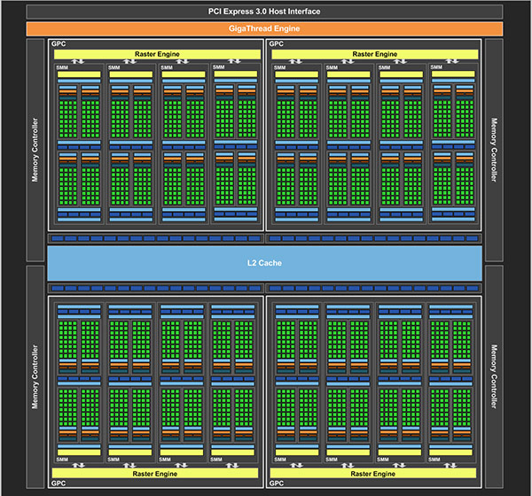
The GeForce GTX 980 is based on the new GM204 GPU, based on Nvidia’s latest Maxwell architecture. The GPU is split into four Graphics Processing Clusters (GPCs) and each GPC has four Streaming Multiprocessor Maxwell (SMM) units, which adds up to 2048 CUDA cores. The GTX 970 is based on the same GM204 GPU, but has fewer units enabled, i.e. 13 SMMs for a total of 1664 CUDA cores. The rest of the specification includes 2MB of L2 cache, 64 ROPs, 128 TMUs and a 256-bit memory interface.
Maxwell GPUs have been optimized to consume as little power as possible and deliver a significant efficiency improvement over Kepler products.
The Maxwell architecture was spawned through a number of advances developed for the Tegra K1. Efficiency is crucial in SoC GPUs and mobile parts. Sales data shows that the gaming laptop market is growing at a staggering pace and it has been doing so for more than five years. Power efficient GPUs have a huge market beyond desktop gaming and Maxwell will eventually make its mark on the mobile segment as well.
Before we move on to more details let’s refresh our memory.
Nvidia launched the GK110 in May 2013 as the Geforce GTX 780 that came with 2304 CUDA cores, 863MHz base GPU clock, 192 texture mapping units (TMUs), 48 render output units (ROPs) and 3GB of GDDR5 memory running on a 384-bit memory bus. The GK110 is split into five GPCs and for the GTX 780 Nvidia enabled 12 out of a total of 15 available SMXs (192 CUDA cores per SMX). Six ROP partitions handle up to eight pixels per clock, adding up to 48 ROP units. Specification wise the GTX 780 ended up with 50% more CUDA cores than its predecessor, the GTX 680, and this among some other things gives the GTX 780 card a significant performance boost, although the GK110 is based on the Kepler architecture used in the GTX 680. The GK104 chip used in the GTX 680 has 1536 CUDA cores. The GTX 780 has a 384-bit bus while the GTX 680 is limited to a 256-bit interface (2048MB memory), but the memory speed on both cards is 6008MHz.
Nvidia launched the GK110B in November 2013 as the Geforce GTX 780 Ti that came with 2880 CUDA cores (all SMXs are enabled resulting in 25 percent more cores than the original GTX 780). The GPU base clock was set at 876MHz. The rest of specification includes 240 texture mapping units (TMUs), 48 render output units (ROPs) and 3GB of GDDR5 memory running on a 384-bit memory bus. The GTX 780 Ti card comes with faster memory (7000MHz effective), compared to the 6008MHz on the GTX 780, resulting in 336GB/s and 288GB/s memory bandwidth respectively.
Now back to GTX 980. The GTX 980 has a 256-bit memory interface (224GB/sec bandwidth) compared to the GTX 780 Ti with 384-bit memory interface (336GB/s bandwidth), but it comes with more memory, 4GB versus 3GB memory on the GTX 780 Ti. To improve the effectiveness of the GPU’s memory bandwidth, the GM204 features a new compression engine which can further reduce DRAM bandwidth demands.
To improve performance in high resolution/high AA workloads, the number of ROPs increased to 64, up from 48 ROPs on the GTX 780 Ti. Combined with the GTX 980’s higher clock speeds (Base GPU clock is 1126MHz), the GTX 980’s pixel fill rate is 72 Gpixels/sec compared to 32.2Gpixels/sec in GeForce GTX 680 or 42Gpixels/sec in GeForce GTX 780 Ti.
Nvidia has rebalanced the design of the Maxwell SM (Streaming Multiprocessor) so that its CUDA Cores are fully utilized more often. This saves power and improves performance. The L2 cache is 2MB – four times larger than on the GK104. By incorporating more cache, fewer requests to GPU DRAM are needed; this improves performance and reduces the GPU’s power consumption.