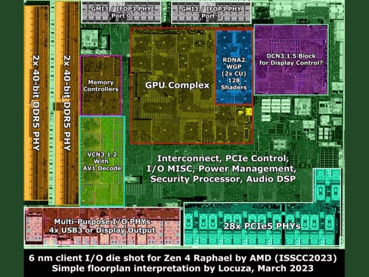
According to Toms Hardware AMD said that Zen 4 uses three nodes: the 5 nm node for the CCD, the 6 nm node for the IO die, and the 7 nm node for the V-Cache.
The V-Cache sits over the middle of the CCD, and the eight cores flank the sides.
This apparently caused the outfit some difficulties when it stacked one node onto another during its recent ISSCC presentation. Both the 7950X3D and the original 5800X3D have their V-Caches positioned over their regular L3 caches to allow them to be connected. The arrangement keeps the V-Cache away from the heat produced by the cores. While the V-Cache fits over the L3 cache in the 5800X3D, it overlaps with the L2 caches on the edges of the cores in the 7950X3D.
The problem was that AMD doubled the amount of L2 cache in each core from 0.5 MB in Zen 3 to 1 MB in Zen 4. It said it worked around the additional space constraints by punching holes through the L2 caches for the through-silicon vias (TSVs) that deliver power to the V-Cache. The signal TSVs still come from the controller in the centre of the CCD, but AMD tweaked them too to reduce their footprint by half.
The Zen 4 L2 cache is larger because of its larger capacity and the TSVs passing through it.
AMD said it shrunk the V-Cache from 41 mm2 to 36 mm2 but maintained the 4.7 B transistors. TSMC fabricates the cache on a new version of the 7 nm node that it developed, especially for SRAM. As a result, the V-Cache has 32 per cent more transistors per square millimetre than the CCD despite the CCD being manufactured on the much smaller 5 nm node.
All this meant that AMD increased bandwidth by 25 per cent to 2.5 TB/s.