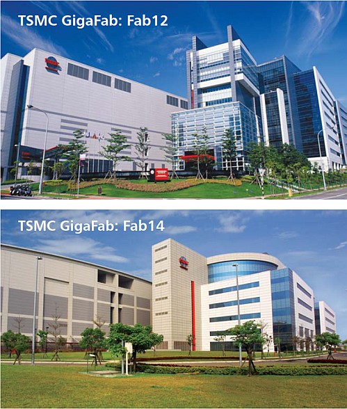
According to several Taiwanese manufacturing equipment suppliers, TSMC has been readying itself for some sizable expansions of its Fab 12 and Fab 14 facilities beginning in the second half of next year. These are the company’s 45nm production sites where it currently produces a significant portion of 12-inch (300mm) wafers. The sources also expect a ramp-up of total wafers to increase 70,000 per month in 2010.
TSMC has been busy at work for a large variety of its customers, particularly those in the GPU sector. The company is expected to invest up to a total of $6 billion for a fifth-phase expansion of Fab 12 and a fourth-phase expansion of Fab 14 respectively. This is all coming from a company that initially slowed down its expansion of total 12-inch capacity amid an economic downturn and reversed this scenario in Q2 2009 to accelerate expansion once again.
Recently issued company filings with the Taiwan Stock Exchange suggest that the company has already expended a total of roughly $193 million on seven purchases of machinery equipment between October 6th and October 27th. In perspective, it’s equipment purchases for Q3 2009 totaled roughly $1.65 billion. The company plans to hold an investors conference sometime today to discuss its Q3 2009 results.
Keep in mind that both Fab 12 and Fab 14 are currently used for 45nm fabrications and are internally referred to be the company’s “GigaFabs” as they can deliver wafers at lower costs than its smaller fabs. However, this is not to say that they won’t be used for more advanced fabrication processes down the road. As stated back in August, TSMC has already announced three 28nm Hi-K process nodes scheduled to enter risk production throughout 2010 beginning in the first quarter.


