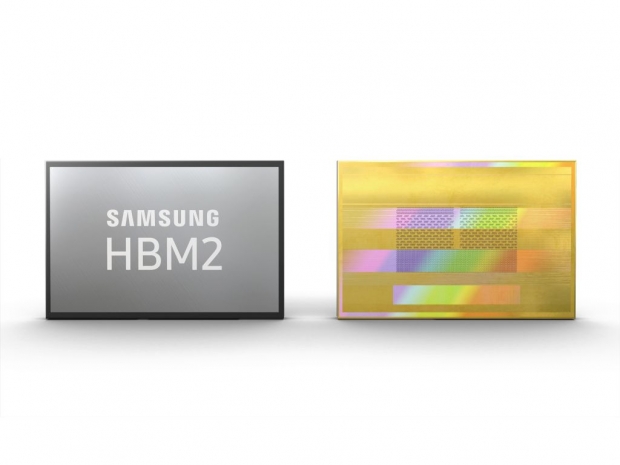
Unlike the first generation Samsung HBM2, codename Flarebolt, which peaked at 2.0Gbps, the new Samsung 8GB HBM2 chips, codenamed Aquabolt, operate at higher 2.4Gbps data rate per pin and are made with a new TSV design and thermal control technologies.
Aimed to be used for supercomputing, AI, and graphics processing, the new 8GB HMB2 uses eight 8Gb HBM2 dies, connected in a vertical stack by using over 5,000 TSVs (Through Silicon Via's) per die.
According to Samsung, the 8GB HBM2 package peaks at 307.2 GB/s of bandwidth, which is 9.6 times faster than on an 8Gb GDDR5 chip. By using four HBM2 packages, it is possible to achieve a 1.2TBps bandwidth, which is a 50 percent improvement compared to standard 1.6Gbps HBM2 chips.
In order to hit 2.4Gbps data rate at rather impressive 1.2V, Samsung had to minimize the collateral clock skew by applying some new TSV technologies. Samsung has also increased the number of thermal bumps between HBM2 dies, enabling better thermal control and added an additional protective layer at the bottom, increasing the overall package strength.
While we do not know when these chips will appear on actual products, Samsung claims that it will supply the new 2nd generation 8GB HBM2 chips to its global IT customers.


