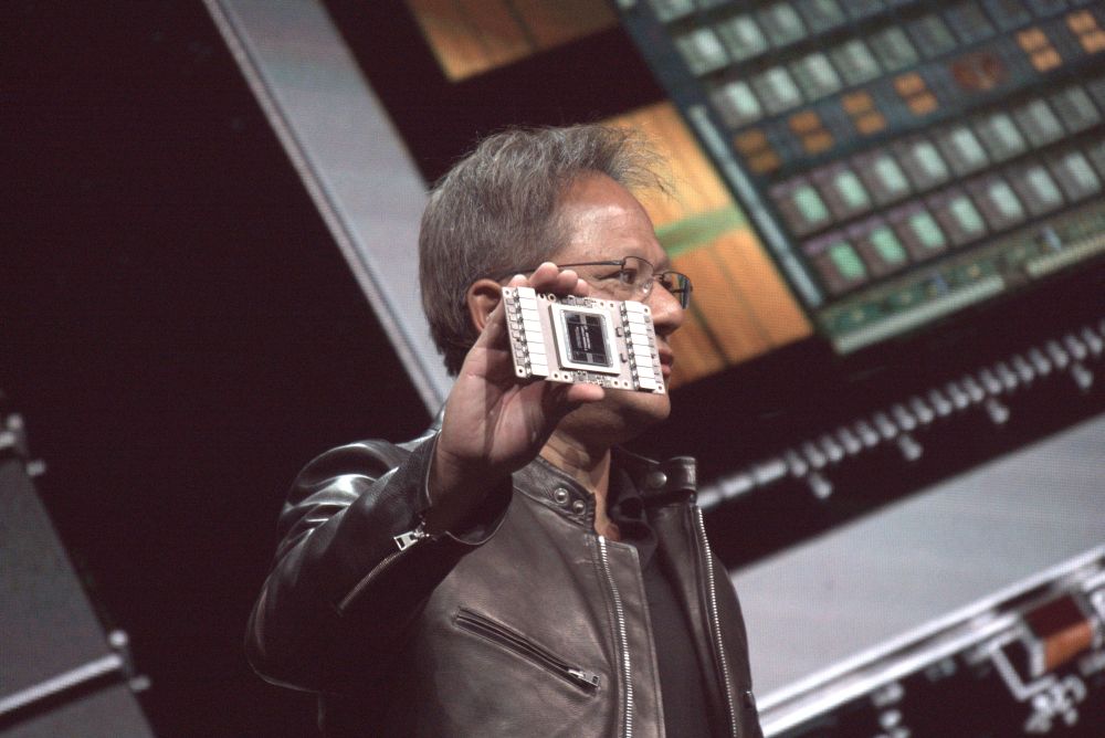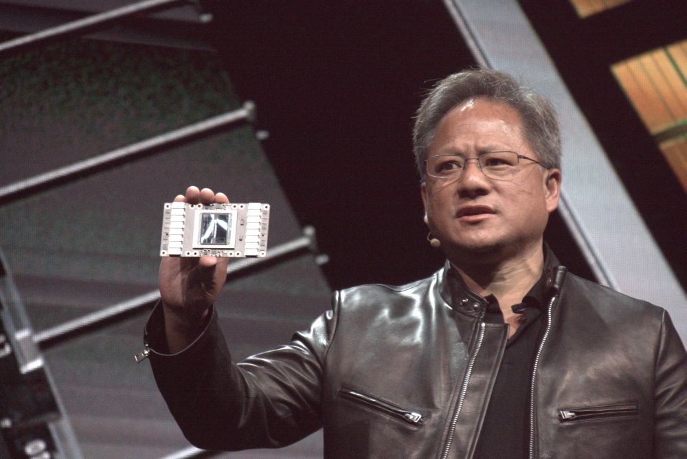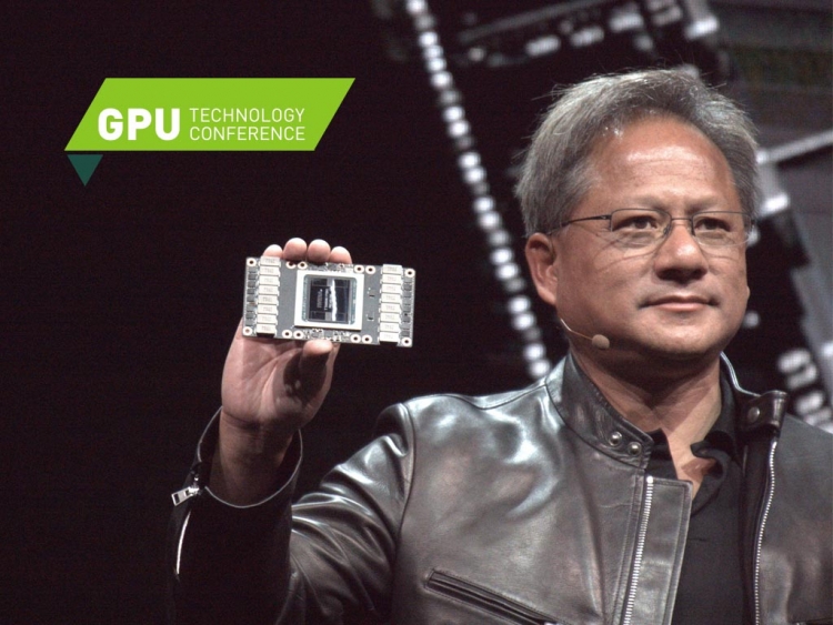
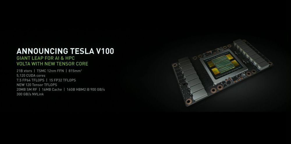
This is the 21 billion transistor core manufactured in TSMCs 12 FFN nanometer process. This is a huge chip, we are talking about 815 mm2. Jensen Huang the CEO of Nvidia compared the die size to the size of an Apple watch.
Nvidia spent three billion of its R&D budget to get to this point, and this is the first of many Volta GPUs and processors. Volta has 5120 Cuda cores and can perform 7.5 FP64 TFLOPS or 15 FP32 TFLOPS.
Nvidia has a special part of silicon here, a die dedicated to a Tensor core. There are 120 Tensor TFLOPS units. The chip is made to be the best in artificial intelligence and deep learning.
The Tesla V100 has 20 MB SM RF with 16GB cache. The memory of choice is the 16GB HBM2 at 900 GB/s and support for 300 GB/s NVlink.
Pascal P100 had 7.1 Billion transistors and came with 3584 Cuda processors. You can tell that the transistor number can be attributed to these new functional units called Tensor units will increase performance in deep learning and AI applications.
We will get back with a few more details after the Q&A that happens in the next few hours.