Image credit: VentureBeat.com
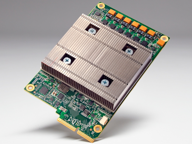
Google says its new Tensor Processing Unit, or TPU, is capable of delivering an order of magnitude higher performance-per-watt “than all commercially available GPUs and FPGAs.” The new accelerator unit is specifically built and custom designed for machine learning tasks. In fact, Google engineer Norm Jouppi says in a company blog post that the TPU accelerators have been running in company datacenters for more than a year, with at least one order of magnitude better performance-per-watt for machine learning tasks requiring reduced computational precision, such as deep learning and object recognition.
The name “Tensor Processing Unit” stems from the accelerator’s original application purpose – Tensor Flow, an open-source software library for computing very large mathematical datasets and interpreting them using visual graphs. The software was originally developed by Google’s Brain Team, a 12-month academic program specializing in machine learning, linguistics, data visualization and neural networks.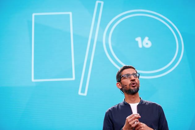
Google CEO Sundar Pichai at I/O 2016 (via Yahoo Finance)
According to company CEO Sundar Pichai, the TPU accelerators will never replace CPUs and GPUs but they can speed up machine learning processes with a fraction of the power draw required by other ASICs. One drawback, however, is that ASICs such as Google’s TPU are traditionally designed for highly-specific workloads. In this case, the applications are TensorFlow and Cloud Machine Learning Alpha, which computes mathematical derivatives and other numerical datasets and allows more tolerance for reduced precision (see: half-precision FP16). Currently, only GPUs and newer CPUs (Intel Haswell and later) support half-precision calculations in TensorFlow. This processing mode is useful for deep learning by reducing memory usage of a neural network, delivers twice the performance of FP32, and allows training and deployment of larger networks over time.
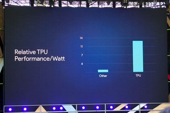
Image credit: VentureBeat.com
“TPU is tailored to machine learning applications, allowing the chip to be more tolerant of reduced computational precision, which means it requires fewer transistors per operation. Because of this, we can squeeze more operations per second into the silicon, use more sophisticated and powerful machine learning models and apply these models more quickly, so users get more intelligent results more rapidly. A board with a TPU fits into a hard disk drive slot in our data center racks.”
Since the gradual slowing of Moore’s Law around mid-2012 (Intel’s last 2D planar architecture launch), scientists have been fervently attempting to defy the laws of atomic-level physics in order to justify the scalability of three-dimensional processor designs over the next two decades. While may claim that tri-gate CPU and FPGA designs will scale at the nanometer level for at least another seven years, Google is now claiming that its TPU will effectively bring 2023 performance-per-watt levels into the present for machine learning applications. The new accelerators will effectively skip three generations worth of Moore’s Law (roughly 2.5 years each), but they are little more than application-specific chips (ASICs) for “playing back” deep learning data. On the other hand, CPU and GPU clusters will still be required to discover and generate most underlying neural network algorithms by sifting through large, near-endless datasets.
Currently, Google uses TPUs to improve web search results using its RankBrain algorithm and to improve the overall accuracy and quality of Street View, maps and navigation routes in general. For now, however, Google senior vice president Urs Hölzle says the company doesn’t need to have TPUs inside every server rack just yet. The company has also ruled out the idea of making TPUs separately available for corporate and enterprise purchases.
According to Diane Greene, Google’s enterprise chief, one reason for this strategy has to do with the company’s cloud-centric business model. It would rather see its customers rent space for deep learning computations on its cloud-based machine learning datacenters (see: Cloud Machine Learning Alpha and pricing) – which require no front-end user maintenance while hardware upgrades (CPUs, GPUs and TPUs) are all performed on Google’s end by qualified engineering and IT staff. While this approach is arguably on the authoritarian side, it gives the company more leverage over some core cloud-focused business segments where research and development in deep learning are concerned. Consequentially, with the performance numbers Google announced today, we should expect some of the company’ competitors to offer deep learning ASICs in retail for consumer and enterprise use in the near future.