On Tuesday at Nvidia’s 2016 GPU Technology Conference in San Jose, California, company CEO Jen-Hsun Huang took the stage and announced Tesla P100, the world’s most powerful workstation based on Pascal, its new 16-nanometer FinFET architecture.
Nvidia's GP100, based on 16nm Pascal architecture
The chip has a stunning 15 billion transistors, up from the 8 billion found in last year’s Tesla M40 and 7.1 billion from the Tesla K40 in 2013. Nvidia claims the total chip has 150 billion transistors, so there are at least another 135 billion transistors in the wafer and memory dies.
After the keynote, we had the opportunity to attend a session called “Inside Pascal,” hosted by Lars Nyland, a senior Nvidia architect who worked on Pascal, and Mark Harris, Nvidia’s chief technologist for GPU computing.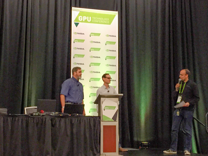
Lars Nyland (left), Senior GPU Architect and Mark Harris (center), Chief Technologist of GPU Computing
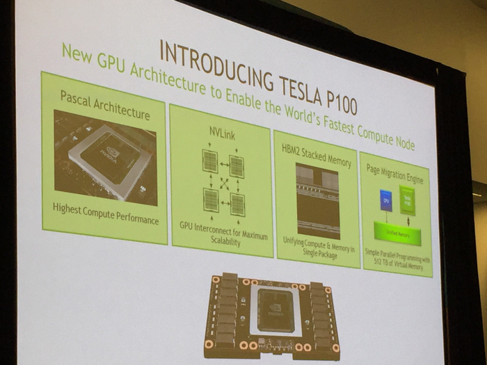
The presentation was packed with details regarding Nvidia's architectural optimizations from Maxwell to Pascal, most notably a page migration engine, NVLINK, and the migration to stacked HBM2 for unifying compute and memory in a single package.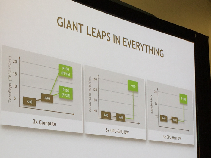
The trend at this year's GPU Technology Conference is deep learning by far, and the sake of architectural improvement, Nvidia has focused a majority of its efforts on optimizing Pascal for deep learning situations where FP64 double-precision math isn't necessarily as important as crunching high volumes of single-precision data. On the other hand, Nvidia does not want to abandon data scientists around the world who rely heavily on double-precision calculations for astrophysics, particle simulations and other scientific studies like it did with Maxwell (see: 0.2 Tflop/s double-precision and 7 Tflop/s single-precision):
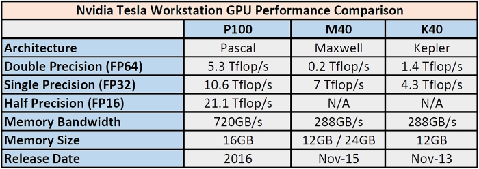
Nvidia Tesla Workstation GPU Performance Comparison (2013 - 2016). Larger image here.
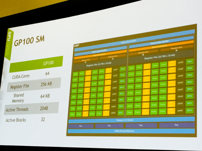
The GP100 has 64 single-precision (FP32) cores, while Maxwell and Kepler SMs were built with 128 and 192 single-precision (FP32) cores each.
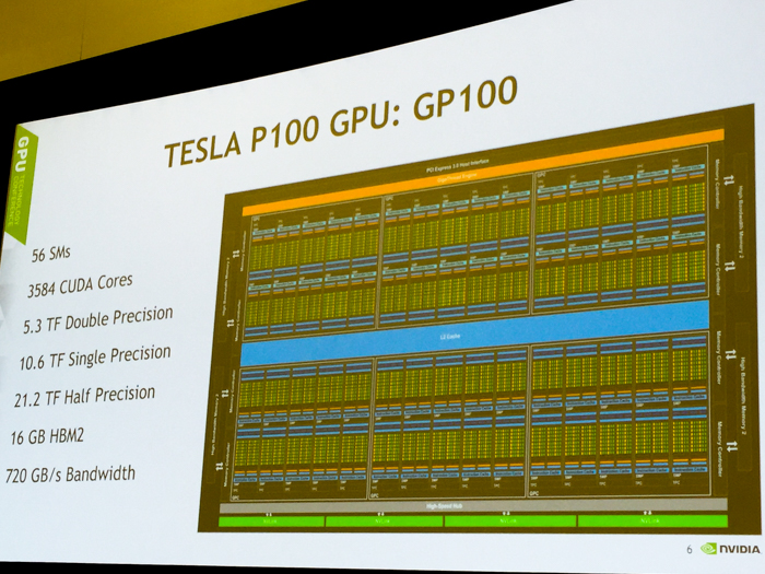
The new GP100 core is composed of 56 streaming multiprocessors (SMs) out of 60 total. This results in 3,584 CUDA cores and 224 texture units instead of 3,840 cores and 240 textures units if all SMs were enabled.
We are more likely to see a variant like this in the second-generation iteration of Pascal which should be announced sometime next year. We are not sure if this was a result of yield issues, but only having 4 SMs disabled is actually not bad for a chip that is 610mm2 with 64 CUDA cores per SM unit.
Meanwhile, the register file size per core is at 256KB, the same as Maxwell and Kepler, but retains only half the amount of CUDA cores per SM (64 instead of 128). The other difference is that the GP100 SMs are partitioned into two processing blocks - they have 32 single-precision CUDA Cores, an instruction buffer, a warp scheduler, and two dispatch units.
"While TSMC’s 16nm Fin-FET manufacturing process plays an important role, many GPU architectural modifications were also implemented to further reduce power consumption while maintaining high performance," explains Mark Harris in Nvidia's blog post on Pascal.
Nvidia's Pascal GP100 block diagram with the all 3,840 cores and 60 SM units (perhaps a future version of Pascal will have all SMs enabled)
“The cores are your most important resource on the SM, and if you aren’t using them, you are wasting resources on your chip,” says Nyland. “So we started with the Maxwell SM and cut it in half. We also doubled the number of warps.”
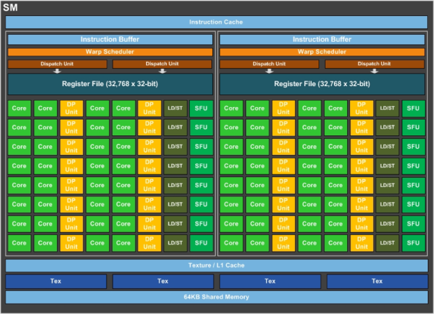
Nvidia Pascal GP100 Streaming Multiprocessor (SM) Diagram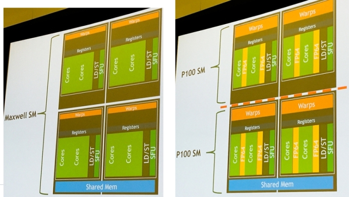
28nm Maxwell SM units (left) vs. 16nm Pascal SM units (right)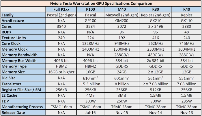
Nvidia Tesla Workstation GPU Specification Comparison (2013 - 2016). Larger image here.
In addition to double and single-precision floating point calculations, Nvidia is introducing support for a new "half-precision" mode for applications including deep learning training, radio astronomy, sensor data and image processing.
"Unlike other technical computing applications that require high-precision floating-point computation, deep neural network architectures have a natural resilience to errors due to the backpropagation algorithm used in their training," explains Harris. "Storing FP16 data compared to higher precision FP32 or FP64 reduces memory usage of the neural network, allowing training and deployment of larger networks. Using FP16 computation improves performance up to 2x compared to FP32 arithmetic, and similarly FP16 data transfers take less time than FP32 or FP64 transfers."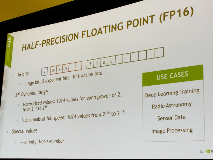
Nvidia NVLINK - Up to 160GB/s GPU-to-GPU bandwidth and 40GB/s GPU-to-CPU bandwidth
“Pascal is the result of thousands of people spending 3 years of hard work to do an amazing thing," said CEO Jen-Hsun Huang during the 2016 GTC opening keynote. “The processor is so fast, the communications between them has to be just as fast. So that’s why we created NVLINK.”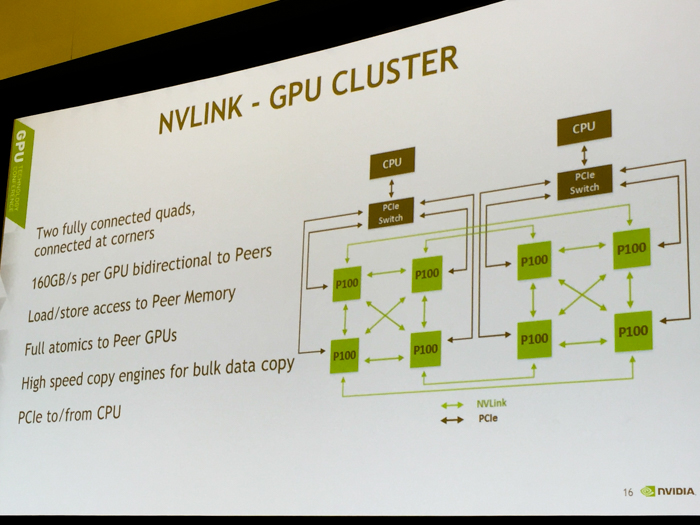
Nvidia's NVLINK uses the company's new High-Speed Signaling interconnect (NVHS). NVHS transmits data over a differential pair running at up to 20GB/s. Eight of these differential 20GB/s connections form a 160GB/s “Sub-Link” that sends data in one direction, and two sub-links—one for each direction—form a “Link” that connects two processors (GPU-to-GPU or GPU-to-CPU).
The proprietary interconnect offers substantially more bandwidth than a PCI-Express 3.0 connection with 16 lanes and is fully compatible with CUDA to support shared memory and multiprocessing workloads.
In English, this means that Nvidia GPUs can now directly communciate with one another, execute data directly in the memory of another GPU and access memory registries from remote GPU memory addresses.
Pascal's NVLINK has up to 94 percent bandwidth efficiency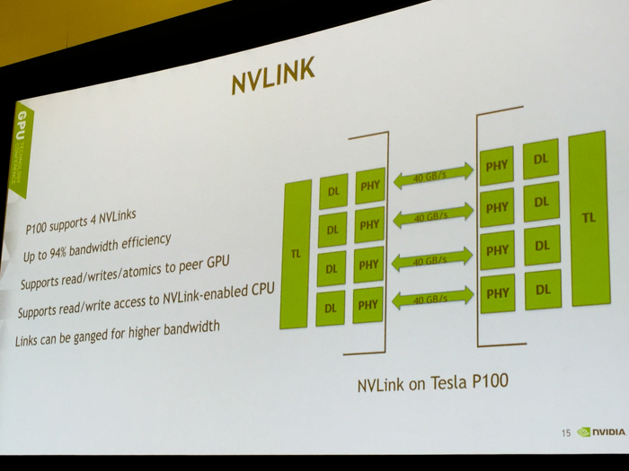
With Pascal's first-generation of NVLINK, we are looking at up to 94 percent bandwidth efficiency, which is incredible when compared to SLI.
“By having more registers, we can have higher occupancy,” says Nyland. “With shared memory, we have double the bandwidth and there is more access to the memory. This results in increased utilization of cores.” The result is up to 160GB/s interconnect bandwidth over NVLINK, the company’s new proprietary GPU-to-GPU and GPU-to-CPU high-speed interconnect for enterprise servers. Read and write access to an NVLINK-enabled CPU is also supported."
Only supports IBM Power Series RISC-based CPUs for now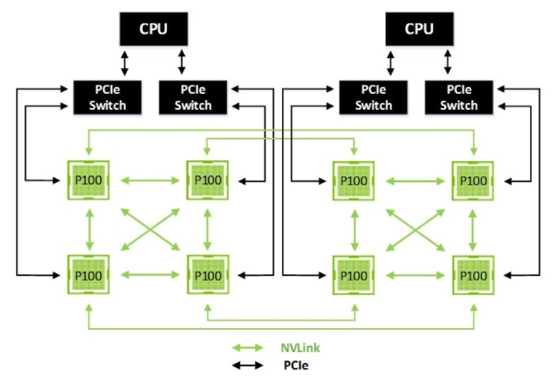
Even with all these great GPU-to-GPU and GPU-to-CPU performance details and numbers, the biggest letdown by far is that Nvidia’s bi-directional NVLINK is still not compatible with x86 processors for the time being. This means that enthusiasts and system builders will not be able to use Nvidia’s high speed 40GB/s GPU-to-CPU link and it will be limited to servers running upcoming IBM RISC-based Power CPUs.