The new standard is expected to run circles around GDDR5, offer up to 95-percent surface area savings on GPUs and allow faster responsiveness for High Performance Computing (HPC) tasks and deep learning supercomputing clusters.
As we mentioned last week, AMD’s 28nm Fiji GPU lineup (Radeon Fury Series) was one of the first to use JEDEC’s High Bandwidth Memory (HBM) DRAM standard. This first-generation HBM standard was limited to 128GB/s (1Gbps per pin) using 4-high TSV stacks across a 1024-bit interface at 1.2v. Now, JEDEC’s updated “JESD235A” HBM2 standard runs 256GB/s and supports 2-high, 4-high and 8-high TSV stacks across a 1024-bit interface at 1.2v and divided into 8 channels on each DRAM stack.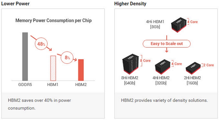
Source: JEDEC (via WCCFTech)
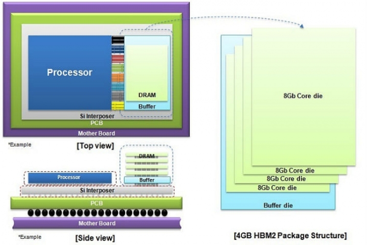
Now, Samsung has created a 20nm 4GB High Bandwidth Memory 2 (HBM2) package with four 8Gb core dies stacked on top of a buffer die at the bottom. These five layers are then vertically interconnected by over 5,000 Through-silicon via (TSV) holes and microbumps. This package contains more than 36 times more holes than an 8Gb TSV DDR4 package. Samsung claims this design offers “a dramatic improvement in data transmission performance compared to typical wire-bonding based packages.”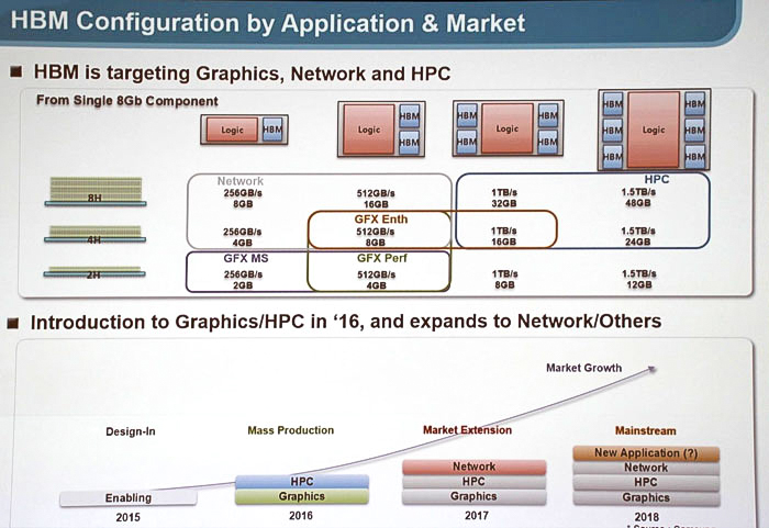
Source: ComputerBase
Like its predecessor, HBM 2 uses an interposer interface to route connections from the GPU to memory. In short, this 4GB HBM2 package can deliver as much as 256GB/s of bandwidth. This is double the bandwidth of first-generation HBM and a seven-fold increase over a 36GB/s 4GB GDDR5 chip, which currently has the fastest data speed-per-pin at 9Gbps. The main difference over HBM1 is that HBM2 offers more DRAM per stack and higher throughput. Samsung’s 4GB HBM2 also doubles bandwidth-per-watt over a 4Gb GDDR5 chip and uses Error-Correcting Code (ECC) for high reliability.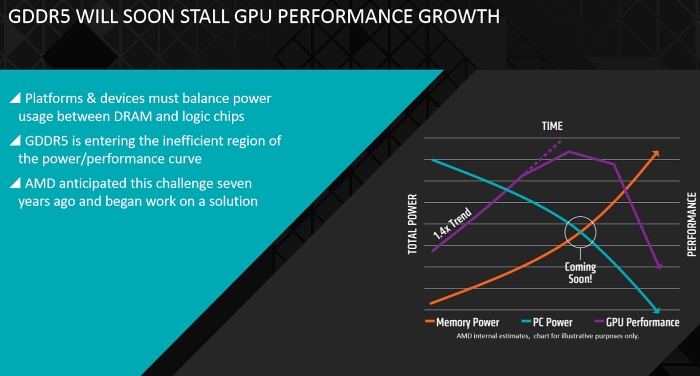
Source: AMD
As AMD mentioned in May 2015, GDDR5 is entering an inefficient region on the “power-to-performance” curve and has called the interposer architecture found in High Bandwidth Memory a “revolution in chip design.” In 2015, the company partnered with Hynix for its 28nm Radeon Fury Series lineup on HBM1 and has recently confirmed that its upcoming 16nm FinFET Polaris GPU lineup will feature both GDDR5 and HBM2 memory technologies. AMD has decided to go with both DRAM configurations because the current HBM cost structure is still too high to implement in all of its next-generation GPUs. Nevertheless, its high-end Polaris models are expected to ship with up to 16GB HBM2 packages, offering peak bandwidth of 1TB/s.
As it looks now, Nvidia has the choice to go with either Samsung HBM2 or SKHynix HBM2 for its Pascal GPU lineup arriving later this year. The consumer GPU series is expected to ship with up to 16GB of 20nm HBM2 memory (four 4GB packages), offering effective memory bandwidth of 1TB/s. Samsung is committed to producing an 8GB HBM2 package this year for use in next-generation enthusiast and workstation graphics cards. On the other hand, AMD will likely stick with either first-gen or second-gen SKHynix HBM, as they helped AMD develop the new memory architecture in the first place. on Nvidia's end, we hope to have more information around GTC 2016 in April.
“By mass producing next-generation HBM2 DRAM, we can contribute much more to the rapid adoption of next-generation HPC systems by global IT companies,” said Sewon Chun, senior vice president, Memory Marketing, Samsung Electronics. “Also, in using our 3D memory technology here, we can more proactively cope with the multifaceted needs of global IT, while at the same time strengthening the foundation for future growth of the DRAM market.”
This density improvement with HBM2 also translates to much smaller GPUs, with reference designs offering as much as 95-percent space savings compared to current GDDR5-based GPUs. At the very least, we can expect to see Samsung’s upcoming 20nm 8GB HBM2 packages in next-generation Quadro and FirePro workstation GPUs.