Index
- Nvidia Geforce GTX 1070 Founders Edition review
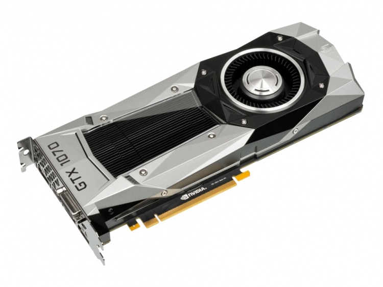
- Hardware - Inside Nvidia's Founders Edition
- Geforce GTX 1070 Specifications
- Power efficiency and design
- Nvidia's Pascal GP104
- HDR display gaming now supported
- H.264 and HEVC playback on Geforce Pascal
- Single, double and half-precision performance
- PCI-E 3.0 x8 and PCI-E 3.0 x16 bandwidth
- Test setup
- Results - Fallout 4
- Results - Far Cry 4
- Results - No Man's Sky
- Results - The Elder Scrolls V: Skyrim
- Results - Just Cause 3
- Nvidia GPU Boost 3.0
- Conclusion
- All Pages
Lower voltage, less transistor leakage, and a higher transistor density
During the official Geforce GTX 1080 and 1070 announcement back in May, CEO Jen-Hsun Huang noted that the company’s engineers have made extensive improvements to the power design and circuitry of its 10-series lineup. Where the Geforce GTX 980 was rated at a 209-millivolt peak-to-peak power efficiency, the GTX 1080 could reach peak-to-peak efficiency at 120-millivolts.
Additionally, GTX 970 idle voltage is 0.856v and Boost voltage is 1.218v, while GTX 1070 idle voltage is 0.625v and Boost voltage is 1.062v. The transition from 28nm transistors to 14nm FinFET is showing some noticeable gains for voltage efficiency, though Nvidia has previously noted that there is a steeper frequency and voltage curve using the 14nm FinFET design.
In terms of the power variance, Jen-Hsun says “with a 1V input, 100mV is all we see. We want to deliver that level of power and current across our entire operating range of GPUs.”
The Geforce GTX 1070 is designed with a 150W TDP, up five watts from the 145W-rated GTX 970. However, the Pascal-based performance card only requires a single 8-pin PCI-E power connector, while the GTX 970 requires dual 6-pin connectors. Maximum GPU temperature has also dropped from a rated 98C with the GTX 970 to 94C with the GTX 1070.