The chip is expected to launch in a few months, and although it is still based on GlobalFoundries’ 28nm node, it still has a number of new features.
Playing the SoC card
What sets Carrizo apart from previous AMD APUs is the fact that it will feature Excavator CPU cores, GCN graphics cores and the Fusion Control Hub (or chipset) in one chip. In that respect, it’s more like a Kabini than a Kaveri, but more advanced – as Carrizo will be the first true HSA part.
The chip has been in the works for a while, and AMD announced it in November, in two flavours – Carrizo and Carrizo-L. Carrizo is expected to launch sometime in Q2 2015, so we expect the first products to show up in time for Computex.
AMD Carrizo highlights
Naturally, the use of the 28nm node is bound to make a lot of people sceptical, and it probably should. However, AMD and Nvidia have already proven that big performance gains are possible on 28n, with Mullins and Maxwell silicon.
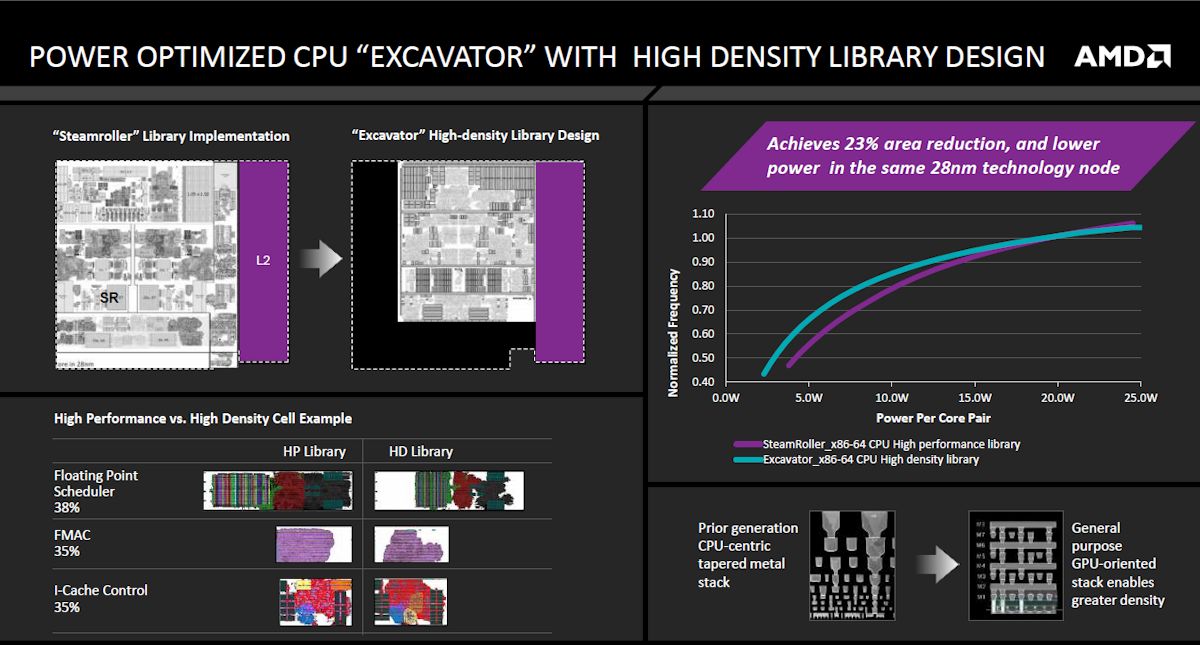
AMD claims the new high density design library results in 29% more transistors than Kaveri, with a whopping 3.1 billion transistors on the same die area. Excavator cores are said to offer a 5% IPC gain, but they need 40% less power and take up 23% less area than Kaveri’s Steamroller cores.
The GPU sports H.265 support and beats Kaveri in transcode performance by a factor of 3.5x. Carrizo’s GPU is based on GCN 1.3 cores and supports DirectX 12 and Mantle APIs.
Carrizo efficiency gains
Power efficiency has been improved too, so AMD expects a 20% improvement over Kaveri, along with a “double-digit” increase in performance and battery life.
While it is based on the 28nm process, design optimisations have reduced leakage by 18%, enabling a 10% clock bump over Kaveri at the same power. The CPU uses 19% less power than Kaveri, while the GPU is 10% more efficient.
AMD also has new low-power states, which help the chip deliver an overall reduction in power consumption of 40%. Carrizo will need just 1.5W in idle mode. Perhaps more importantly, SKUs optimised for thin and light notebooks will end up at about 10W, which is a very impressive improvement.
What the future holds for AMD APUs
One of AMD’s slides also revealed a number of new features in development, and coming in future APU parts.
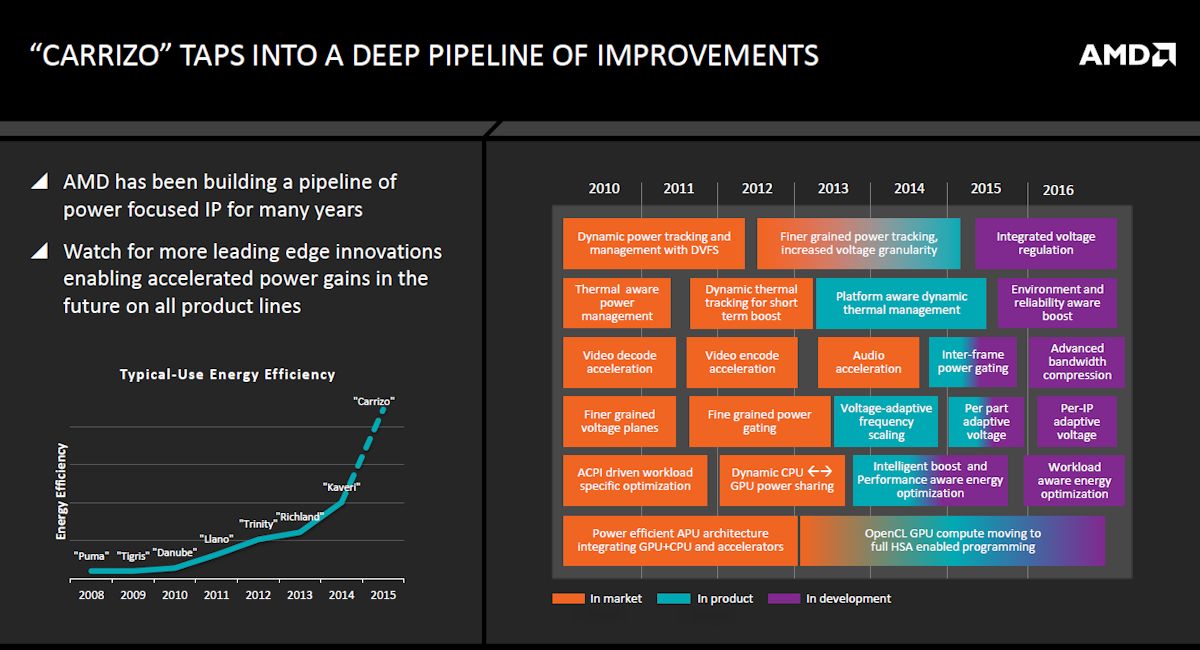
Some of them are coming on Carrizo, but quite a few will show up later, in 2016 and beyond. These include advanced bandwidth compression on the GPU side, which sounds rather interesting, especially with fast DDR4 RAM. Integrated voltage regulation, workload aware energy optimization, and per-IP adaptive voltage could also make a big difference in future AMD chips.
Hopefully AMD won’t run into execution problems, which would be a pity since Samsung and GlobalFoundries finally have a competitive FinFET node that’s practically ready for prime time.