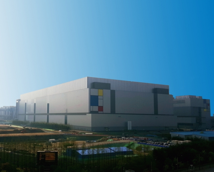
Just a week ago, Qualcomm announced that it plans to launch its 7nm Snapdragon X24 modem and have it ready for customer trials this year. This is as far as we are aware the first 7nm chip ever publicly announced and Qualcomm has taped out the chip. The chip is real, not a piece of a PowerPoint roadmap.Samsung Electronics will make the Qualcomm's 7nm ULV chips in its foundry manufacturing line located in Hwaseong, Korea.
Now the new announcement is about the unnamed future 5G mobile chipset.
7nm EUV is a big deal
EUV, that is to say, Extreme Ultra Violet lithography process is needed once we get to 7nm or 5nm. Guess what, according to Qualcomm and Samsung, this is happening this year. Since Intel has yet to launch its 10nm parts, it is hard to imagine that Intel can have 7nm chips ready next year. Qualcomm on the other hands has shipped millions of 10nm based Snapdragon 835 and it is ramping and shipping millions of Snapdragon 845 as we speak, both 10nm.
The 7nm LPP (Low Power Plus) will enable a smaller chip footprint leaving more space for OEMs. This should result in larger batteries, slimmer designs and probably more space for antennas too. You will need some extra antennas for 5G to complement the new frequencies. That will be needed to get to 4.5 Gbps or faster speeds.
The 7nm LPP chip will enable better battery life and higher frequencies. Phones of the future will be faster in both wireless and compute performance, this is the natural way of semiconductors.
The 7nm LPP with EUV was announced in May 2017, and less than a year later, Samsung is revealing that Qualcomm is one of its big customers. TSMC might reportedly be late to the 7nm game. Samsung believes that EUV lithography deployment will break the barriers of Moore’s Law scaling, paving the way for single nanometer semiconductor technology generations. The single nanometer just sounds much smaller than 7nm.
From 65nm to 7nm in a decade
The first Snapdragon QSD8650 launched in Q4 2008, not even 10 years ago, and it was a 65nm chip. We went from 65nm to 45nm with Snapdragon 2 and 3. The Snapdragon 4 was a 28nm chip. Snapdragon 800, 801 and 805 were 28nm, while Snapdragon 808 and 810 were the first 20nm.
Snapdragon 820 and 821 were the company’s first 14nm parts and as we've said many times before, the Snapdragon 835 and current 845 are 10nm parts. The mobile industry went from 65nm to 7nm in a decade.
If you compare Samsung’s 7LPP EUV with 10nm FinFET not only greatly reduces the process complexity with fewer process steps and better yield, but also allows up to a 40 percent increase in area efficiency with 10 percent higher performance and up to 35 percent lower power consumption.
You can expect that the next generation 5G chipset from Qualcomm (most likely Snapdragon 855 ed.) to pack significantly more transistors, let's say up to 40 percent on the same die space, and get at least 10 percent higher performance while having 35 percent lower power consumption. The 35 percent lower power consumption can translate directly to significantly better battery life.
RK Chunduru, senior vice president, supply chain and procurement, Qualcomm Technologies said: “We are excited to lead the 5G mobile industry together with Samsung. Using 7nm LPP EUV, our new generation of Snapdragon 5G mobile chipsets will take advantage of the process improvements and advanced chip design to improve the user experience of future devices.”
Charlie Bae, executive vice president of foundry sales and marketing team at Samsung Electronics said: “We are pleased to continue to expand our foundry relationship with Qualcomm Technologies in 5G technologies using our EUV process technology. This collaboration is an important milestone for our foundry business as it signifies confidence in Samsung’s leading process technology.”