
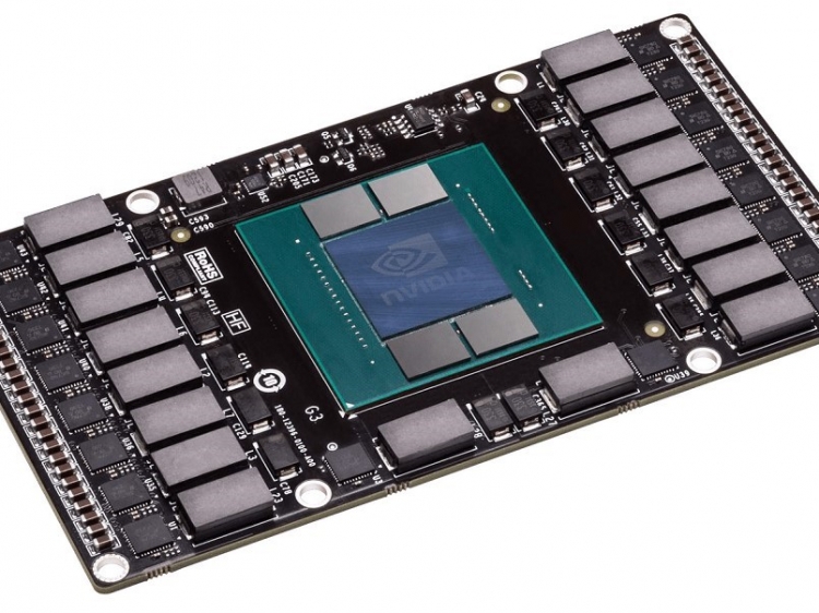
The researchers found that the reason is due to the adoption of such products by Nvidia's Tesla P100 accelerator and Quadro GP 100 graphics card as well as AMD's Radeon Vega chip.
In addition to HBM-based products, there is a variant version of HMC (hybrid memory cube) chips. While both HBM and HMC solutions are made with a similar vertical stacking process to integrate multilayer DRAM devices on a base logic die, the HBM is more like a 2.5D stacked-die packaging solution, and the HMC is closer to a 3D stacked-die packaging process.
SK Hynix and Samsung Electronics are using wafer level packaging (WLP) process to fabricate HBM2-based chips, TSMC is using chip-on-wafer-on-substrate for HBM2 devices. Micron Technology and Chipzilla focus mainly on HMC-based products.
Intel's deep-learning chip, Lake Crest, which came following its acquisition of Nervana, has come with HMB2. This indicates that HBM-based architecture will be the primary development direction of memory solutions for HPC solutions by GPU vendors, Digitimes Research thinks.
The high packaging cost and compatibility are likely to continue to affect the applications and popularity the HBM2 chips, Digitimes Research added.