It will show up in the cloud soon but OEM's will get it in Q1 2017 due to demand, is what Jensen just said to the GTC 2016 audience.
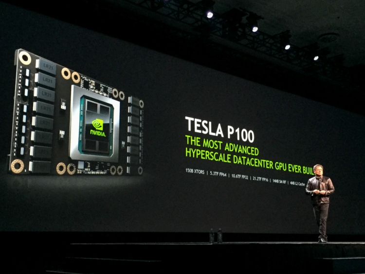
Be aware that this is not a Geforce product, but it is what Geforce P100 would roughly look like. Some things got confirmed like G100. Jensen talked that this is 610mm2 chip, largest ever built by them, and it features 150 billion transistors. The GPU itself has 15.3 billion transistors, and this has been recently confirmed by Nvidia.
The only way that this number is real is that if you add the GPU transistors and Samsung HMB2 memory chips that are sitting on the same silicon. Remember P100 uses HBM 2, the next generation memory from Samsung.
This is a 5.3 teraflops in FP64, 10.6 teraflops in PF32, and 21.3 teraflops in FP16 solution built with TSMC 16nm FinFET manufacturing process and using Samsung HBM 2.0 memory.