Index
Review: High factory overclock and silent cooler
Nvidia’s Geforce GTX 980 and GTX 970 are extremely powerful and successful graphics cards, and now with the GTX 960 the power efficient Maxwell architecture is available to mainstream consumers.
Maxwell even made its way into the mobile Tegra X1 SoC and there is no doubt that the architecture is extremely power efficient, despite its reliance on the mature 28nm node.
Nvidia launched the Geforce GTX 960 describing it as a “sweet spot” graphics card. Traditionally Nvidia “sweet spot” cards as the 60-series models such as the GTX 460, 560, 660, 760 and so on. They tend to offer a good price/performance ratio and the current generation can run most titles at 1080p with high detail settings. The suggested MSRP for the GTX 960 is 200€.
Nvidia gave its partners the green light to launch custom GTX 960 designs from day one, so we are already seeing factory overclocked cards with custom coolers and PCBs. The GTX 960 offers AIBs a chance to show what they can do, since the card is a good overclocker, doesn’t require a lot of power and does not generate much heat.
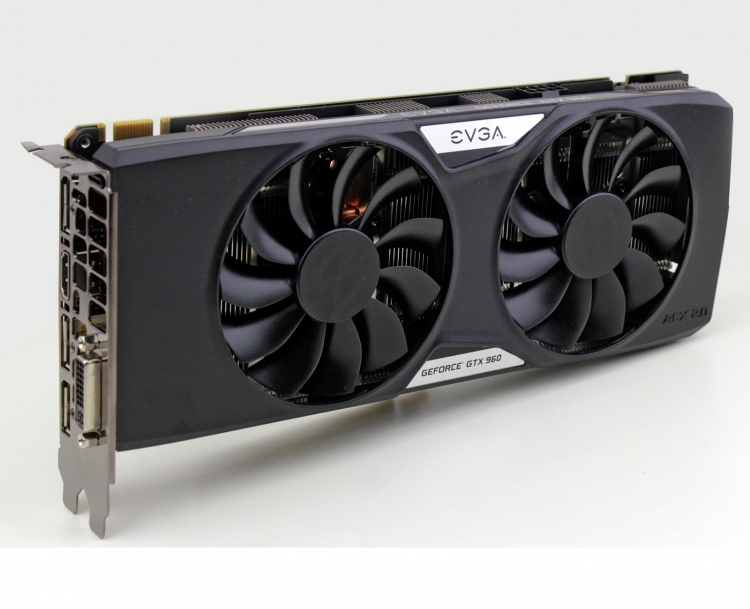
As one of Nvidia’s premier partners, EVGA was one of the first players to launch a number of custom cards. While most AIB partners are offering one or two 960-series cards, EVGA is going a step further, or a few steps with no less than six different GTX 960 cards. Today we will take a look at one of them – the EVGA Geforce GTX 960 SuperSC ACX 2.0+ (Part Number: 02G-P4-2966-KR) with EVGA’s new dual-fan cooler.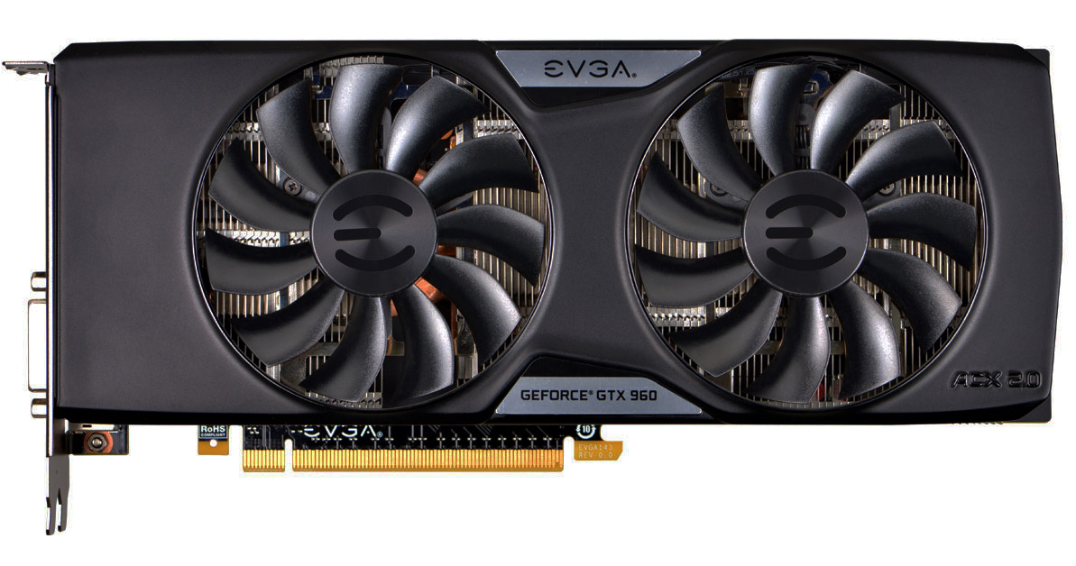
The GTX 960 SuperSC ACX 2.0+works at a base clock of 1279MHz, while the reference GPU base clock is 1126MHz. Nvidia's GPU Boost 2.0 takes the average GPU clock to 1178MHz for the reference GPU and to 1342MHz for the SuperSC card. Note that the actual Boost clock will vary on different machines and in different titles.
EVGA did not change the memory clock. The GTX 960 SuperSC ACX 2.0+features 2GB of GDDR5 memory clocked at 1752MHz (7010MHz effective), providing up to 112.16GB/sec of peak memory bandwidth.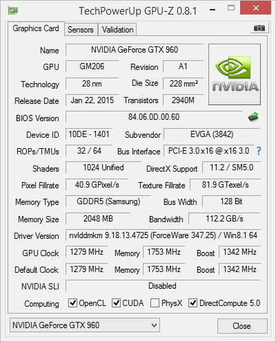
The new ACX 2.0+ cooler is supposed to ensure quiet and cool operation despite the factory overclock, but it should also provide additional overclocking headroom. One 8-pin power connector provides additional power in case the user want to overclock the GPU even further. The reference GTX 960 card uses only one 6-pin power connector.
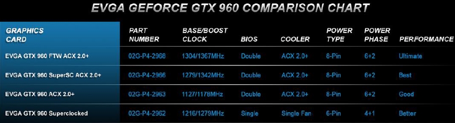
The next photo shows EVGA’s GTX 960 line-up. The GTX 960 FTW is only 25MHz faster than the SuperSC version.
Nvidia designed Maxwell to deliver more efficiency and performance, so the GTX 980, GTX 970 and GTX 960 are vastly more efficient than their Kepler-based predecessors. The GTX 980 has a TDP of 165W, the GTX 970 is rated at 145W, while the GTX 960 has a TDP of 120W.
The old GTX 780 Ti and GTX 780 have a TDP of 250W, while the GTX 760's TDP stands at 170W, the same TDP as the GTX 670. Just like their predecessors the GTX 980 and GTX 970 cards are capable of delivering smooth frame rates at resolutions up to 2560x1600, while the GTX 960 is good for playing at up to the 1920x1080. In case you are planning to build a 4K capable gaming rig, you will have to grab a couple of GTX 980/970 cards. The GTX 960 is mainstream card and it supports SLI, however two GTX 960 will be enough for 4K gaming only in less demanding titles.
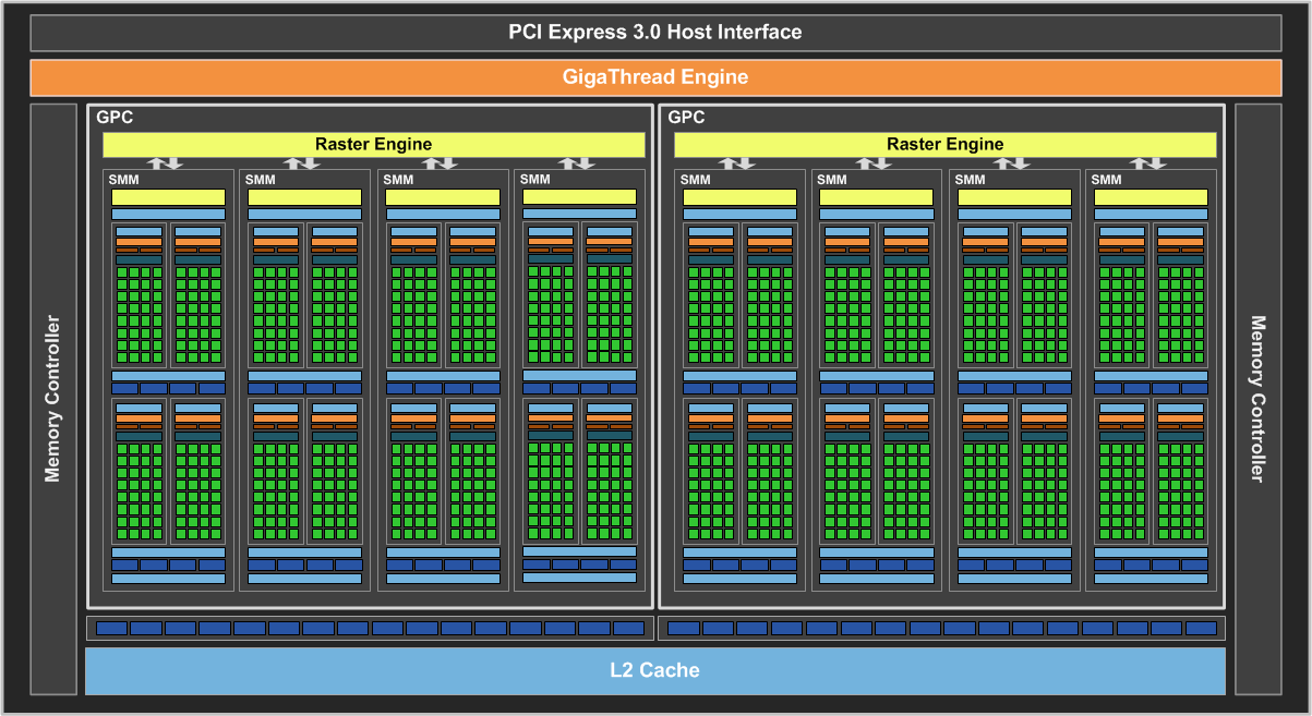
Compared to previous Maxwell products, the GeForce GTX 960 features an entirely new GM206 GPU. It supports all of Maxwell’s new graphics features like VXGI and MFAA, and comes with an advanced video engine.
Like the flagship GeForce GTX 980, the GeForce GTX 960 has a new display engine capable of supporting resolutions up to 5K with up to four simultaneous displays (including support for up to four 4K MST displays). The GeForce GTX 960 also supports HDMI 2.0.
Because of its low power design, some potential GeForce GTX 960 users may wish to use this GPU in their home theater PC (HTPC). Therefore to satisfy the needs of this niche audience, one new addition that’s been added to GM206 is support for H.265 (HEVC) encoding and decoding. GTX 980’s NVENC video engine offers native support for H.265 encode only, no decode. With the amount of 4K content expected to explode in the coming years, GM206 also adds native support for HDCP 2.2 content protection over HDMI.
The GM206 GPU
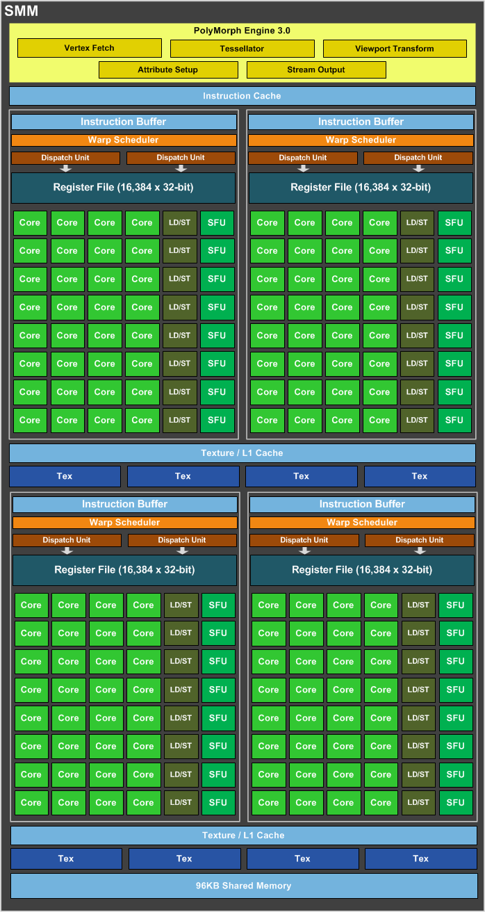
The GM206 GPU used in the GeForce GTX 960 features all the key architectural innovations first introduced in the GeForce GTX 980. Maxwell GPUs feature a new SM design that’s been tailored to improve efficiency.
The Maxwell SMM is partitioned into four distinct 32-CUDA core processing blocks (128 CUDA cores total per SM), each with its own dedicated resources for scheduling and instruction buffering. By giving each processing block its own dedicated resources for instruction scheduling and dispatch, Nvidia is able to keep the GPU’s CUDA cores fully utilized more often, improving workload efficiency and reducing wasted power.
To improve the efficiency of the GPU’s onboard caches, Nvidia has also made a number of changes to the cache hierarchy in Maxwell. Each of GM206’s SMM units features its own dedicated 96KB shared memory, while the L1/texture caching functions are combined into a 24KB pool of memory per pair of processing blocks (48KB per SMM). Prior generation Kepler GPUs had a smaller 64KB shared memory function that was also shared as L1 cache.
As a result of these changes, each GM206 CUDA core is able to deliver roughly 1.4x more performance per core compared to a GK106 Kepler CUDA core (the direct predecessor of GM206), and 2x the performance per watt.
Memory Subsystem
The memory subsystem of GM206 has also been revamped. Nvidia’s third-generation delta color compression engine offers new modes for color compression, allowing the GPU to use its available memory bandwidth more effectively. When combined with the aforementioned caching improvements in the Maxwell SM, GM206 uses roughly 25% fewer bytes per frame compared to prior generation Kepler GPUs. This means that from the perspective of the GPU core, a Kepler-style memory system running at 9.3Gbps would provide effective bandwidth similar to the bandwidth that Maxwell’s enhanced memory system provides.
The memory subsystem of GeForce GTX 960 consists of two 64-bit memory controllers (128-bit) with 2GB of GDDR5 memory. The 128-bit, 7Gbps memory interface is able to effectively provide slightly more bandwidth than its direct predecessor (148.8GB/sec effective in GTX 960 vs 144.2GB/sec in GTX 660).