In case you missed it earlier, the GV100 GPU is made on TSMC's new 12nm FinFET manufacturing process and packs 21 billion transistors on 815mm2 silicon. The GPU packs 5120 CUDA cores with 640 new Tensor Cores, offering 112 TFLOPs of Tensor performance - meant for deep learning - and it comes with 6MB of L2 cache, 16GB of HBM2 memory on a 4096-bit memory interface.
The PCIe Tesla V100 offers 14 TFLOPs of single-precision compute performance, 28 TFLOPs of half-precision and 7 TFLOPs (1/2 rate) of double-precision compute performance with Tensor cores providing 120 TFLOPs of performance for deep learning.
Due to a lower 250W TDP, mostly due to lower GPU clocks, compared to the SXM2 version of the Tesla V100 accelerator, the PCIe version of the Tesla V100 offers slightly lower compute and Tensor performance but it is still a massive improvement over the earlier available Tesla P100 PCIe accelerator which offered 9.3 TFLOPs of single-precision compute performance.
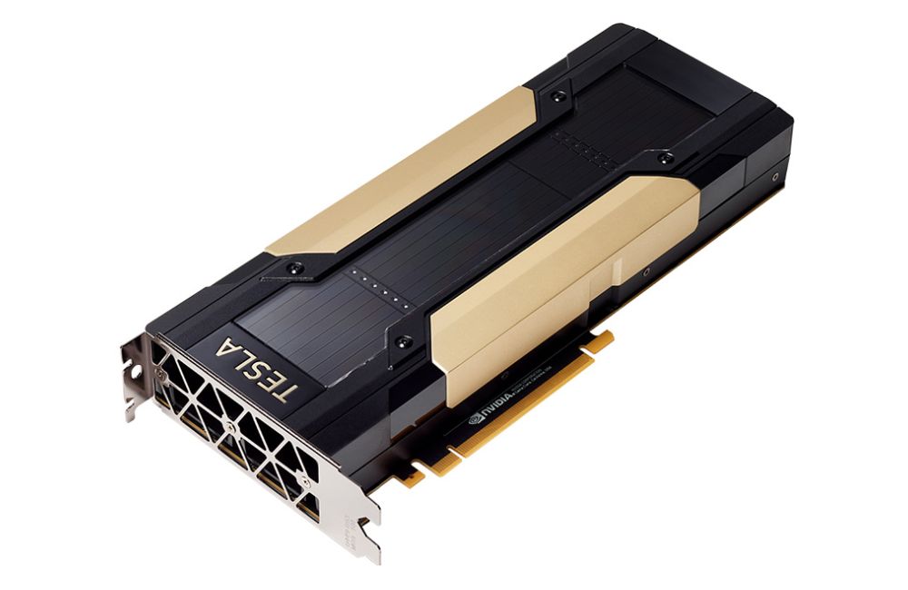
The PCIe version of the Tesla V100 retains passive cooling, which was a standard for all Tesla accelerators, including the upcoming SXM2 form-factor Tesla V100 and earlier available Tesla P100 in both PCIe and SXM2 form-factor.
According to Nvidia, the PCIe Tesla V100 accelerator should be available later this year and usual suspects, like HP, are likely to offer systems based on the Nvidia V100 accelerator.