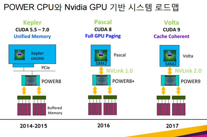
IBM launched its Power8 lineup of superscalar symmetric multiprocessors back in August 2013 at the Hot Chips conference, and the first systems became available in August 2014. The announcement was significant because it signaled the beginning of a continuing partnership between IBM and Nvidia to develop GPU-accelerated IBM server systems, beginning with the Tesla K40 GPU.
The result was an HPC “tag-team” where IBM’s Power8 architecture, a 12-core chip with 96MB of embedded memory, would eventually go on to power Nvidia’s next-generation Pascal architecture which debuted in April 2016 at the company’s GPU Technology Conference.
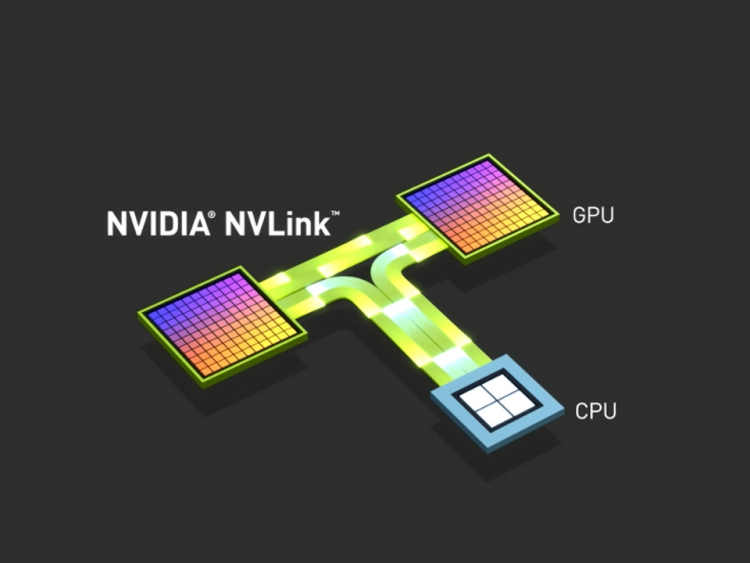
NVLINK, first announced in March 2014, uses a proprietary High-Speed Signaling interconnect (NVHS) developed by Nvidia. The company says NVHS transmits data over a differential pair running at up to 20Gbps, so eight of these differential 20Gbps connections will form a 160Gbps “Sub-Link” that sends data in one direction. Two sub-links—one for each direction—will form a 320Gbps, or 40GB/s bi-directional “Link” that connects processors together in a mesh framework (GPU-to-GPU or GPU-to-CPU).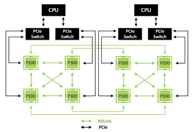
Nvidia cube mesh diagram with CPU-to-GPU interconnects
NVLINK lanes upgrade from 20Gbps to 25Gbps
IBM is projecting its Power9 servers to be available beginning in the middle of 2017, with PCWorld reporting that the new processor lineup will include support for NVLINK 2.0 technology. Each NVLINK lane will communicate at 25Gbps, up from 20Gbps in the first iteration. With eight differential lanes, this translates to a 400Gbps (50GB/s) bi-directional link between CPUs and GPUs, or about 25 percent more performance if the information is correct.
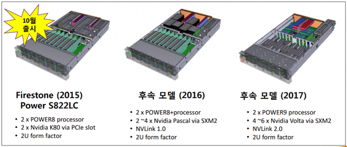
NVLINK 2.0 capable servers arriving next year
Meanwhile, Nvidia has yet to release any NVLINK 2.0-capable GPUs, but a company presentation slide in Korean language suggests that the technology will first appear in Volta GPUs which are also scheduled for release sometime next year. We were originally under the impression that the new GPU architecture would release in 2018, as per Nvidia’s roadmap. But a source hinted last month that Volta would be getting 16nm FinFET treatment and may show up in roughly the same timeframe as AMD’s HBM 2.0-powered Vega sometime in 2017. After all, it is easier for Nvidia to launch sooner if the new architecture is built on the same node as the Pascal lineup.
Source: IBM - Optimizing Data-Centric IT Environments (2015)
Still ahead of PCI-Express 4.0
Nvidia claims that PCI-Express 3.0 (32GB/s with x16 bandwidth) significantly limits a GPU’s ability to access a CPU’s memory system and is about “four to five times slower” than its proprietary standard. Even PCI-Express 4.0, releasing later in 2017, is limited to 64GB/s on a slot with x16 bandwidth.
To put this in perspective, Nvidia’s Tesla P100 Accelerator uses four 40GB/s NVLINK ports to connect clusters of GPUs and CPUs, for a total of 160GB/s of bandwidth.
Source: IBM - Optimizing Data-Centric IT Environments (2015)
With a generational NVLINK upgrade from 40GB/s to 50GB/s bi-directional links, the company could release a future Volta-based GPU with four 50GB/s NVLINK ports totaling of 200GB/s of bandwidth, well above and beyond the specifications of the new PCI-Express standard.