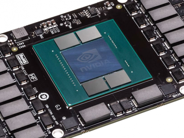
It is also the first Nvidia GPU to use second-generation High Bandwidth Memory (HBM2). Nvidia is skipping HBM1, which will be used on AMD’s upcoming Fiji GPU. However, AMD’s decision to proceed with an HBM1 design will give it a head start, since Fiji is about to launch in a week or so, while Pascal is still a couple of quarters away.
The biggest downside to HBM1 is the limited amount of memory that can be integrated in the design, which is why AMD’s flagship Fiji VR card is expected to ship with two GPUs and a total of 8GB of HBM1, 4GB per GPU.
Nvidia’s Pascal on the other hand could address as much as 32GB, although it’s simply not necessary. It might be a possibility on some professional graphics cards, or compute cards, but it would be overkill for gamers.
AMD is expected to transition to HBM2 next year.