
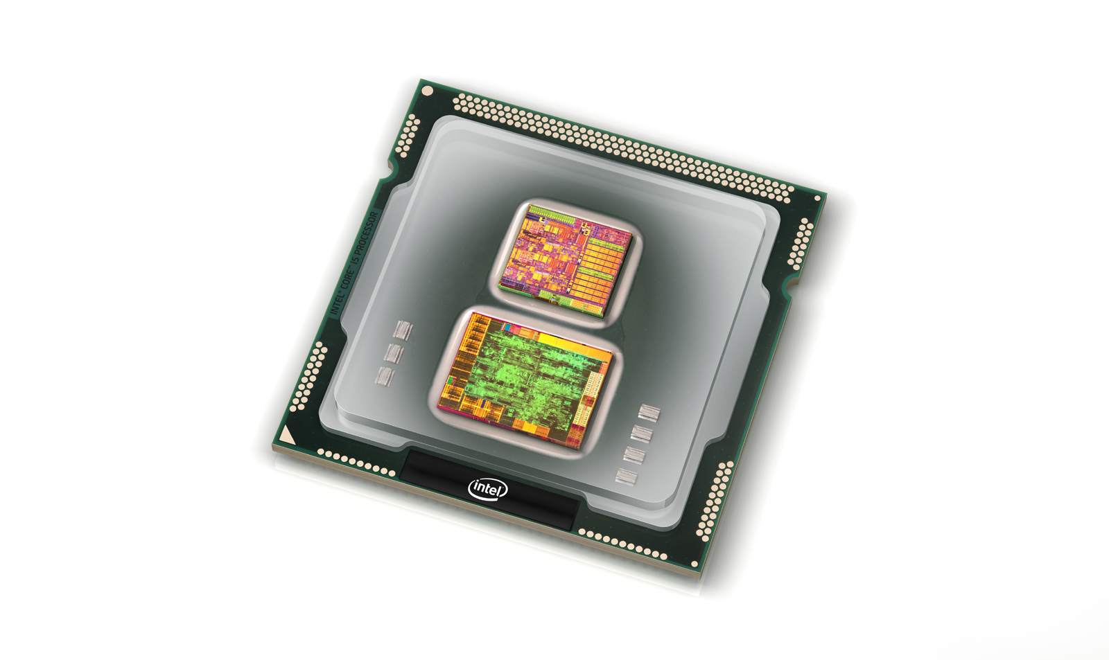
Intel Clarkdale CPU + GPU architecture (January 2010)
Fast forward to September 2009, and we observe Intel transferring the rest of its PCH-based "northbridge" functions into the CPU die, beginning with 45nm Lynnfield. Fast forward again to January 2010, and we observe some new dedicated GPU logic in Intel's chip packages as multi-chip modules (MCMs) with separate CPU and GPU dies, beginning with Clarkdale (32nm CPU + 45nm GPU). Fast forward to January 2011, and we now observe a complete integration of GPU logic and CPU logic on the same die, beginning with 32nm Sandy Bridge.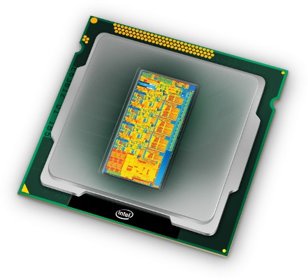
Intel Sandy Bridge integrated CPU / GPU architecture (January 2011)
Beginning with its 22nm Haswell notebook platform in 2013, Intel will take a further step towards full integration of the Platform Controller Hub (PCH) with the CPU for its third-generation lineup of Ultrabooks. The platform is called "Shark Bay" for notebooks and ultrabooks, and it will consist of a single Multi-Chip Module (MCM) package fully integrating the PCH from previous generation 22nm Ivy Bridge (2012) directly into the same die as the 22nm Haswell (2013) CPU. Of course, there will be limitations to this first-generation MCM mobile platform, and that is that mobile Haswell chips will be limited to dual-core models only as there isn't enough room to fit PCH logic and more than two CPU cores in the same package at just 22 nanometers.
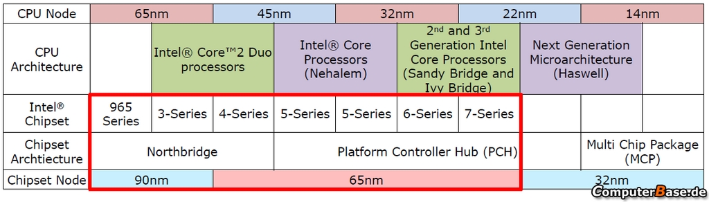
Image source: ComputerBase
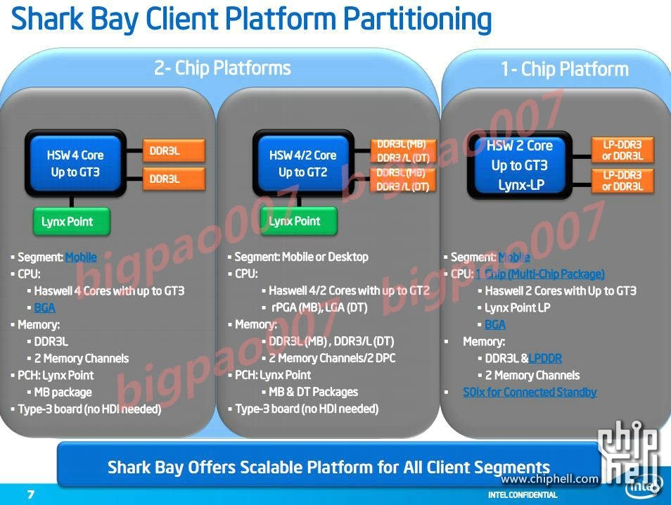
Image source: ChipHell
This is where 14nm Broadwell comes to play. In 2014, Intel will be ready to mass produce on the 14 nanometer process node and we will see full integration of the PCH with quad-core and higher CPU dies. Interestingly enough, for some reason Intel calls its 14nm Broadwell architecture a "true System-on-a-Chip (SoC) platform," and we can't help but disagree with this naming convention.
Image source: ComputerBase (Full size here)
By the textbook definition, a System-on-a-Chip (SoC) is an integrated circuit that integrates all components of a computer's architectural framework into a single chip substrate. However, most desktop / server / enterprise systems are much too complex to fit on a single chip substrate without having to be stacked on top of each other first. There is another word for this type of "stacking" substrate architecture, and it's called a chip-stack Multi-Chip Module (MCM). In other words, it is very likely that Intel is designing a carefully-engineered 14nm Broadwell substrate that allows multiple dies (see: PCH, CPU) to be stacked in a vertical configuration on top of one another, resulting in an MCM footprint much different than that of an SoC.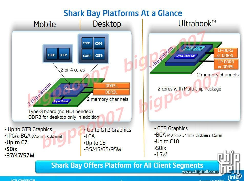
ChipHell: Intel 22nm Haswell single-chip (MCM) mobile architecture overview (right)
So, for Intel to call its third-generation Ultrabook platform based on 22nm Haswell architecture a "true System on a Chip" platform is entirely beyond us. Simply put, the architecture more closely resembles that of a Multi-Chip Module package, possibly a stacked one at that. Nevertheless, we remain hopeful that the company will better address the semantics of its architectural designs in future marketing presentations announcing 14nm Broadwell desktop chips and its fourth-generation Ultrabook platform beginning in 2014.

