Featured Articles

After USA Nvidia’s Shield comes elsewhere

After USA Nvidia’s Shield comes elsewhere

Project Shield, which is now called Nvidia Shield, is up for preorder, at least if you’re in North America. For…

More...
Nvidia won most Haswell high-end notebooks

Nvidia won most Haswell high-end notebooks

Our sources in the Far East are claiming that most Haswell notebooks that are coming out in the next few weeks…

More...
Microsoft officially announces the Xbox One

Microsoft officially announces the Xbox One

As announced earlier, Microsoft has now finally unveiled its next-generation console, the Xbox One. Although it did not shed much light…

More...
AMD poaches more Nvidia talent

AMD poaches more Nvidia talent

AMD has apparently managed to grab yet another high-ranking Nvidian, but this time it was no engineer or developer.

More...
HIS iCooler Turbo HD 7790 reviewed

HIS iCooler Turbo HD 7790 reviewed

Today we’ll take a closer look at a factory overclocked HD 7790, courtesy of HIS. The HIS HD 7790 iCooler Turbo…

More...
Frontpage Slideshow | Copyright © 2006-2010 orks, a business unit of Nuevvo Webware Ltd.
Sunday, 15 April 2012 05:26

Nvidia terminates GeForce GTX 580 production

Written by Jon Worrel

nvidia

40nm Fermi second-gen GF110 reaches EOL

Alas, the day has finally arrived for Nvidia to terminate production of its GeForce 500 Series single-GPU flagship card, the GeForce GTX 580. The card that many enthusiasts all referred to as "GF110" is finally going EOL (end-of-life) as of April 2012.

580-cooler-1

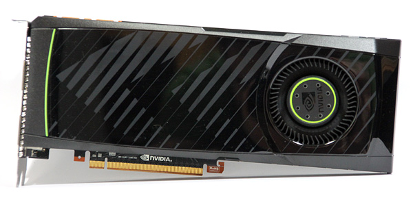
Nvidia's GeForce GTX 580 is based on GF110, a second-generation 40nm Fermi chip that ended up producing noticeably more efficient performance-per-watt over its GeForce 400 Series predecessor, the GeForce GTX 480 (GF100). The secret to the company's improved performance and yields on second-gen GF110 chips ultimately came from a monitoring and rearranging of the transistor paths that caused most of the leakage on first-generation GF100 in real-world environments. As such, many of the segments on Nvidia's ~530mm2 GF100 die were rearranged to better improve efficiency and power consumption, resulting in a slightly smaller 520mm2 GF110 die for the GeForce GTX 580.

As many avid GPU enthusiasts remember, the card was launched on Tuesday, November 9th, 2010 at a suggested MSRP of $499, although many retailers began selling them for around $50 higher at $549.99 and £425, respectively. As of now, the card has been on the market for just over 1 year and 5 months.

Meanwhile, adoption rates of Nvidia's new 28nm Kepler-based GeForce GTX 680 (see: GK104) have been soaring and we expect the company will have some nice margins to play with on this newer, significantly more efficient GPU until it releases the rest of its 28nm Kepler lineup over the remainder of 2012.

Last modified on Tuesday, 17 April 2012 06:58

Jon Worrel

E-mail: This e-mail address is being protected from spambots. You need JavaScript enabled to view it
blog comments powered by Disqus

To be able to post comments please log-in with Disqus


Facebook activity

Latest Commented Articles

Recent Comments