
According to Electronic Times Intel and TSMC’s products are still being processed at 14-nano and 16-nano so Samsung's 10-nano S-RAM, will open the way for a generation of Giga-Smartphones. S-RAM is faster than D-RAM and is used for CPU’s cache memory.
It means that Samsung's 10-nano technology will be mass-produced on full-scale in early 2017. The theory is that 10-nano AP will combine Gigabyte modem chips into one faster chip.
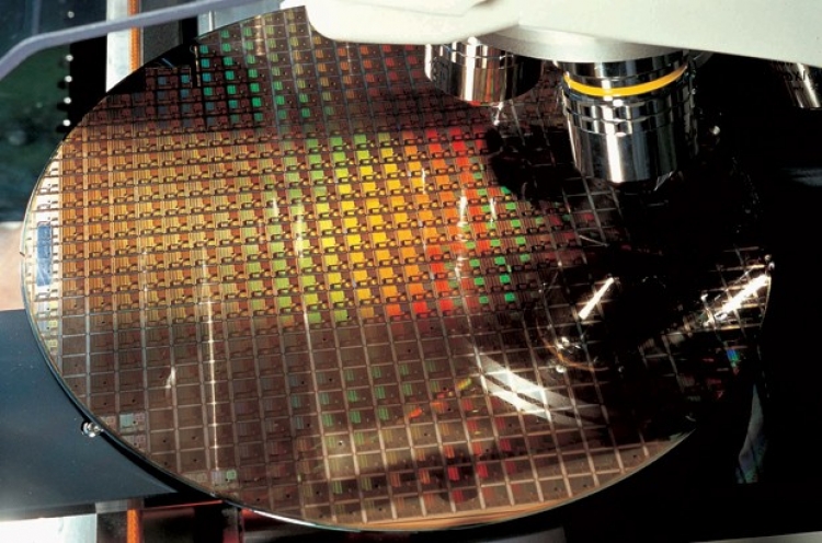
Samsung is showing its plans to the ISSCC. They will have a 128 Megabyte (MB) capacity and a cell area of 0.040 µm2. This compares to the 14-nano S-RAM (0.064 µm2) that Samsung Electronics introduced in the past, its cell area is reduced by 37.5 per cent.
In an ISSCC scientific paper, Samsung said that it built a large-scale fast cache memory in the smallest area. An AP for a smartphone with S-RAM, can minimize Die’s area and improve its performance.
All this means that Samsung Electronics has surpassed Taiwan’s TSMC and developed the next-generation system semiconductor.
Intel postponed its schedule for developing next-generation 10-nano system semiconductor from 2016 to 2017 due to increase of production costs. Samsung Electronics is targeting end of next for commercialising 10-nano processing.
Samsung Electronics has also developed 14-nano flat-surface NAND-Flash, and this is also first ever in industries. Toshiba, Micron and others have announced that after they finish developing 15 to 16-nanos, they are giving up on flat-surface NAND-Flash.
It had been thought that 14-nano NAND-Flash, which reduces area of Floating Gate by about 12.5% compared to 16-nano, will greatly contribute to Samsung Electronics in reducing production cost of NAND by reducing Silicon Die’s area.