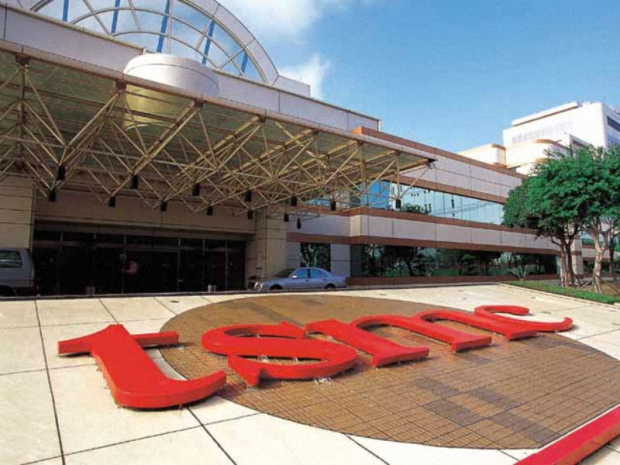
In an interview with Guru3D, Suk Lee, Senior Director at TSMC’s Design Infrastructure Marketing Division, said the 10nm node is “progressing” and the IP validation process started six months earlier than on previous nodes.
This is how Lee outlined TSMC’s schedule:
“We are working with over 10 customers on their 10nm product design. The qualification schedule remains at the end of 2015. We are working with customers on tapeout, and we expect volume production in 2017.”
TSMC’s FinFET learning curve
Lee pointed out that moving from 16nm to 10nm will include some “learning”, but noted that TSMC has already refined FinFET on 16nm, so the transition to 10nm should be smooth.
He said the company was able to “engage very quickly at 10nm” thanks to its work on the 20nm and 16nm FinFET ecosystem. TSMC has already completed certification of 35 EDA tools using ARM CPU cores as the test vehicle.
While Lee was eager to talk about 10nm, he did not wish to disclose any details regarding next generation processes. It is rumoured that TSMC’s next node will be 7nm – Intel is also planning to move to 10nm, followed by 7nm.
Lee said the next generation node will be offered in the 2017-2019 timeframe, adding that Moore’s Law is not going to slow down anytime soon.
20nm was not a mistake
Lee also commented on the somewhat controversial 20nm process, which he described as the “ultimate planar technology”. He said it was a conscious strategy that allowed TSMC to mitigate risk.
Lee explained:
“We had a very advanced metal stack with a set of leading customers who wanted to squeeze every last drop out of planar. So 20nm turned into a great deal of business for us. We didn't have to take on two challenges at the same time—developing this complex metal system and bringing up FinFET.”
By “leading customers”, Lee was obviously referring to Qualcomm and Apple. In fact, back in December our sources told us that Qualcomm was the real reason TSMC decided to go ahead with another planar node.
Lee also added that TSMC gained a lot of valuable experience from the 20nm transition, as the metal system developed for the 20nm node helped make the 16nm FinFET ramp much easier.


