
High Bandwidth Memory (HBM) is what will be used in the GPUs of the future, and at this point the concept hardly needs an introduction. The first generation of HBM will be used in AMD Fiji, a GPU that is expected to come in the next few months.
AMD uses HBM1, Nvidia HBM2
Nvidia will use 2nd generation HBM that will enable its Pascal GPU to get to a whopping 32GB on the highest end card, 2.7 times more than the already impressive 12GB used on Titan X cards.
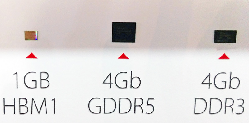
The 4-HI HBM1 has a 1024-bit interface, can handle two prefetch operations per IO and has a maximum bandwidth of 128GB per second. The tRC is 48nm, with tCCD of 2ns (1tCK), and the VDD voltage of 1.2V. For example GDDR5 has 1.35 to 1.5V and a top bandwidth of 28GB/s throughput per chip.
In addition, 4-Hi HBM1 16Gb (2GB per chip) and 8-Hi HBM1 32Gb (8GB per chip) is possible and HBM2 will get double the bandwidth and density. With first generation HBM memory it is at least theoretically possible to design a card with 8GB to 16GB of memory, assuming that the company would be using 4 HBM chips on an interposer, resulting in 512GB/s bandwidth on a four-chip HBM card.
Boosting density and capacity
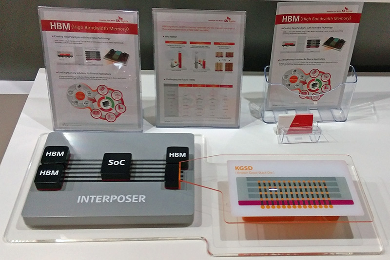
HBM uses Trough Silicon VIA (TSV) technology, as it is stacking the memory cores on top of each other on the same base die. It is amazing that SK Hynix manages to make these layered interconnections trough the silicon. It’s one thing to read research papers about it, but seeing the finished product is something else. As you can see, HBM chips will be significantly smaller than GDDR5 and DDR3 chips.
The HBM1 acts as a stack of eight 2Gb chips, resulting in 16Gb (2GB) per chip, while the second generation HBM doubles the density to 32Gb (4GB) per chip, with 4-Hi HBM2 modules or even 64Gb 8GB with 8-Hi HBM2 memory. This is how Nvidia will be able to get 32GB with four chips on Pascal.
So if you do the math you can get 512GB with four HBM1 chips and 1024GB/s with four HBM2 second-generation chips, which means AMD might have a second generation Fiji with HBM2 and Nvidia will use the same technology on Pascal, sometime in 2016.
In any case, HBM represents the biggest change on the memory front in years. Coupled with new FinFET nodes, 2016 promises to be a very eventful year for the GPU industry.