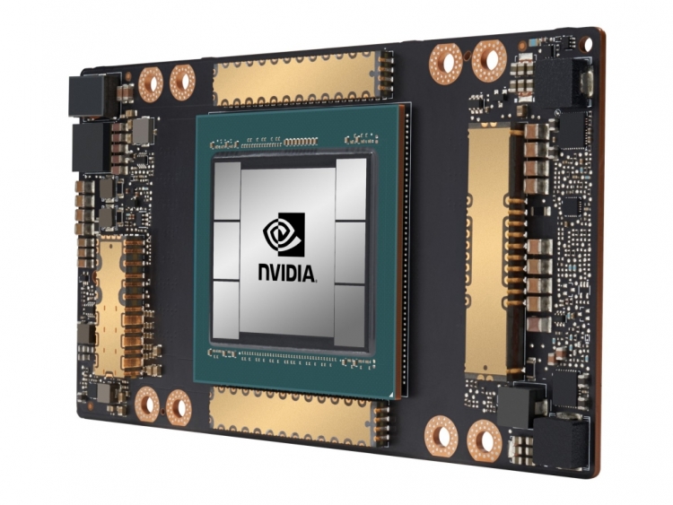
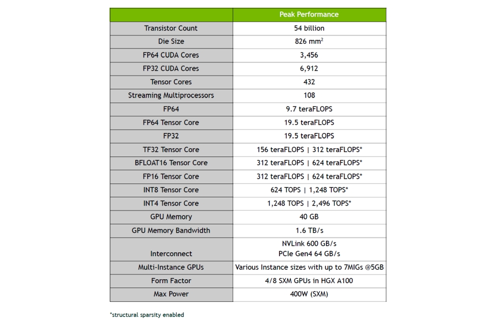
As we already wrote, the A100 Tensor Core GPU is based on the GA100 GPU, which we wrote about earlier, and when compared to the fully enabled GPU, it comes with one less GPC, leaving it with a total of 108 SMs and 6912 FP32 CUDA cores, as well as 432 Tensor Cores, and 40GB of HBM2 on a 5120-bit memory interface with 1.6TB/s of memory bandwidth.
The A100 Tensor Core GPU is a compute beast
The story of the day is the A100 GPU accelerator, or as Nvidia calls it, the A100 Tensor Core GPU. Designed as a successor to the V100, the Ampere-based A100 GPU brings several new features and delivers significantly higher performance in HPC, AI, and data analytics workloads.
According to Nvidia, it also provides strong scaling for GPU compute and AI deep learning (DL) applications both in single- and multi-GPU workstations, servers, clusters, cloud data centers, systems at the edge, and supercomputers.
The A100, which is based on the GA100 GPU, works at up to 1410MHz, packs 7 enabled GPCs, for a total of 108 SMs and 6912 FP32 CUDA cores per GPU.
With this in mind, it also comes with 432 3rd generation Tensor Cores, as well as features 5 HBM2 stacks and 10 512-bit memory controllers, leaving it with 40GB of 1215MHz DDR HBM2 and 5120-bit memory interface for a total of 1.6TB/s of memory bandwidth.
The GPU packs 40960KB of L2 cache with up to 164KB of shared memory size per SM.
The Nvidia A100 comes in SXM4 board form factor and has a TDP of 400W, as well as has the third-generation of NVIDIA high-speed NVLink interconnect with a total of 12 links, leaving it with 600GB/s of total bandwidth, doubling it compared to V100. The A100 also supports PCI Express Gen 4, offering 31.5 GB/sec.
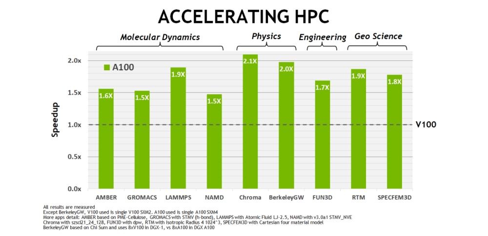
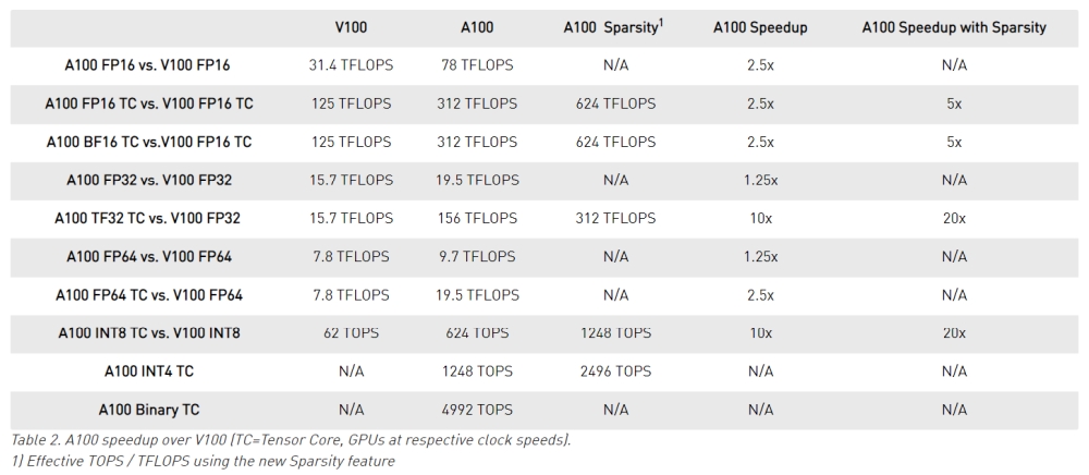
When it comes to compute performance, the A100 does not bring significant improvements in single-precision performance (FP32), peaking at 19.5 TFLOPs, which is not far from 15.7 TFLOPs on the V100, and the double-precision (FP64) compute peaks at 9.7 TFLOPs (7.8 TFLOPs for the V100), but this is where Tensor cores come in.
Tensor Cores are what matters
The Volta-based V100 was only capable of pushing FP16 Tensor computations, peaking at 125 TFLOPs, which is far behind 312 TFLOPs that A100 can achieve. Unlike the V100 640 Tensor Cores, the 432 Tensor Cores in the A100 GPU can do all computations, including FP16, BF16, TF32, FP64, INT8, INT4, and Binary.
The performance gain is incredible with A100 hitting 19.5 TFLOPs for double-precision (FP64), 156 TFLOPs for TF32, and 125 TFLOPs for BF16/FP16 compute performance.
Plenty of other improvements, including the Multi-Instance GPU (MIG)
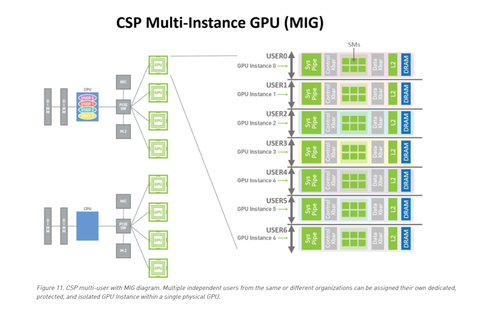
In addition to new architecture improvements, 3rd gen Tensor Cores, more VRAM, large L1 and 40MB of L2 cache, all leading to an impressive compute performance uplift, the A100 GPU will bring several other improvements, like the new Multi-Instance GPU (MIG) feature, which allows the A100 Tensor Core GPU to be securely partitioned into as many as seven separate GPU Instances for CUDA applications.
With MIG, each of those instance's processors have separate and isolated paths through the entire memory system, as well as uniquely assigned on-chip crossbar ports, L2 cache banks, memory controllers, and DRAM address busses. This allows better utilization of the GPU hardware while isolating different clients, like VMs, containers, and processes.
In addition to the MIG, the A100 brings the aforementioned third-generation of NVIDIA high-speed NVLink interconnect with 600GB/s of total bandwidth, support for NVIDIA Magnum IO and Mellanox interconnect solutions, PCIe Gen 4, single root input/output virtualization (SR-IOV), has improved error and fault detection, isolation, and containment, support aforementioned asynchronous copy instruction with asynchronous hardware-accelerated barriers in shared memory, has ask graph acceleration, and more.
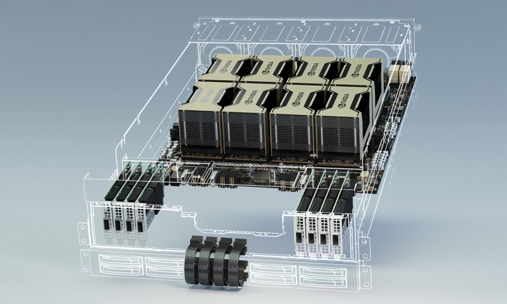
The A100 GPU comes in the DGX A100 AI System
The A100 GPU will be available in Nvidia's DGX A100 AI system which features eight A100 Tensor Core GPUs, providing 5 PFLOPs of AI power, and 320GB of memory for 12.4TB/s of memory bandwidth. It also includes six NVIDIA NVSwitch interconnect fabrics, nine Mellanox ConnectX-6 HDR 200Gb per second network interfaces, 15TB Gen4 NVMe internal storage, and NVIDIA DGX software stack.
The Nvidia DGX A100, which should be immediately available and shipping worldwide, with the first customer being the U.S. Department of Energy’s (DOE) Argonne National Laboratory, starts at $199,000. It will be available through NVIDIA Partner Network resellers worldwide.