
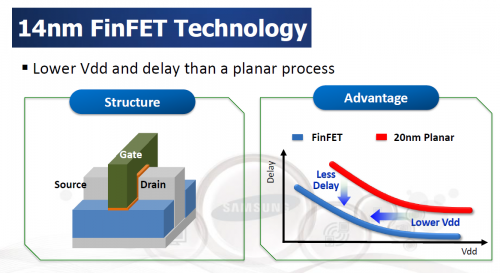
In the first quarter of 2015, the company announced the launch of the Exynos 7 Octa SoC built on the industry’s first-generation 14nm low-power early (LPE) process. Now, Samsung is claiming that new chips made with the second-generation 3D FinFET process have up to 15 percent more performance at 15 percent less power compared to the low-power early (LPE) process found in last year’s Exynos 7 Octa. Samsung is promising “unparalleled performance and power efficiency” for this year’s Exynos 8 Octa SoC and for many of its customers’ SoC designs such as Qualcomm’s 2.2GHz quad-core Snapdragon 820.
Mass production of Samsung’s Exynos 8 Octa 8890 began in Q4 2015. This is the company’s first custom-designed CPU based on the 64-bit ARMv8 architecture. Now, Samsung is taking credit for catapulting its customer Qualcomm onto second-generation 14nm 3D FinFET structures by starting production of its Snapdragon 820 2.2GHz quad-core SoC with Adreno 530 graphics. We can only conclude this will result in a more competitive ARMv8 chip contest in 2016 as last year’s Snapdragon 810 suffered throttling issues and had relatively high power consumption on the 20nm process node.

Source: GSMArena
“We are pleased to start production of our industry-leading, 2nd generation 14nm FinFET process technology that delivers the highest level of performance and power efficiency” said Charlie Bae, Executive Vice President of Sales & Marketing, System LSI Business, Samsung Electronics. “Samsung will continue to offer derivative processes of its advanced 14nm FinFET technology to maintain our technology leadership.”
In this second generation 14nm process, the majority of performance and efficiency gains have been made through improvements in the transistor structure and process optimization. Samsung has overcome scaling limitations by using fully depleted FinFET transistors to enhance its manufacturing capabilities.
Source: Samsung
The term FinFET was originaly coined by Professors Chenming Hu, Tsu-Jae King-Liu and Jeffrey Bokor at the University of California, Berkeley and describes a nonplanar, double-gate transistor built on a silicon-on-insulator (SOI) substrate. However, general technical literature refers to the “FinFET” process as any fin-based, multigate transistor architecture regardless of the number of gates.
Meanwhile, rival Taiwan Semiconductor Manufacturing Company (TSMC) rolled out its low-power compact 16nm FinFET process back in October (with plans to scale down to 10nm later this year). AMD is also utilizing new FinFET improvements at the 14nm process node from GlobalFoundries in its upcoming Zen CPU lineup.
The competition for second-gen 14nm FinFET technology is heating up and rumors are currently circulating that the Samsung-manufactured Qualcomm Snapdragon 820 may be the SoC of choice for the former company's upcoming Galaxy S7 flagship smartphone. The folks at GizBot have spotted the device (SM-G935A) running the Antutu system benchmark and featuring the 2.2GHz quad-core Snapdragon 820, a 5.1-inch 2650x1440p display, 4GB of RAM, 64GB of onboard storage, a 12-megapixel camera, Android 6.0 Marshmallow and the Samsung TouchWiz UI on top.