According to an interview between EE Times and GlobalFoundries CEO Ajit Manocha, the company's exceptionally positive Q4 2011 revenue results will allow the firm to "keep the momentum going" after a year plagued with diffuculties and setbacks. Manocha said that the company would continue to develop its upcoming fabrication plant in Dresden, Germany which will be the site of 32nm, 28nm and 20nm wafer production.
"In addition, we are working on 14nm and 10nm with our [joint development] partners," said Manocha. "Since we do not have the home-grown R&D, we are using a collaborative model of R&D [with our partners]."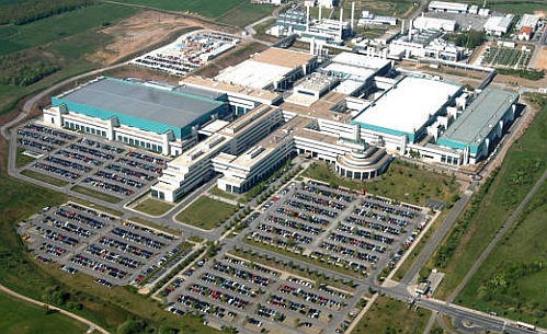
GlobalFoundries fabrication plant in Dresden, Germany
Manocha also made sure to compare his firm's achievements with rival foundry TSMC (Taiwan Semiconductor Manufacturing Company), noting that GlobalFoundries has already shipped over 700,000 High-K Metal Gate (HKMG) wafers on the 32nm process note, whereas TSMC has only shipped "a few thousand" High-K Metal Gate wafers on the 28nm process node. Of course, it is somewhat audacious to compare one company's 32nm shipments with another's 28nm shipments, especially since TSMC has admitted that the majority of its 28nm production relies on Silicon Oxynitride (SiON) and not High-K Metal Gate (HKMG).
The full interview can be found here.
Published in
News
GlobalFoundries prepares for 14nm process node

To be manufactured with Joint Development partners
GlobalFoundries, the world's third largest independent semiconductor foundry, has said that it has already begun planning phases for upcoming 14nm process node technology. This statement marks the first time that the company has publicly announced any 14nm plans, as it has previously only discussed its 16nm process technology which will use EUV lithography techniques.
Tagged under