Index

Review: Fast, pricey and hot
We've been waiting, and waiting and waiting some more, but today the wait is over for the most part. This is probably second most controversial if not the most controversial chip in Nvidia’s history and we must admit we haven’t seen such lousy execution with so many delays since the NV30 days.
You might recall that Fermi was supposed to launch in November, then December and then it was finally pushed for the last days of March. Back in November Nvidia did make an A2 silicon that was ok, but could not clock at desired speeds and the company decided to wait for A3 and make things right.
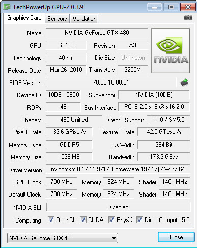
The final GPU clock is 700MHz. Shaders, or GPU CUDA cores as Nvidia calls them, run at 1401MHz and the GDDR5 memory runs at 1848MHz. Its 12 memory chips pack a total of 1536MB of GDDR5 memory. The memory comes from Samsung and and it's designated K4G10325FE-HC04. These can be traced as specified to run at 1250MHz (5000MHz effective). The card also features a CHiL branded voltage regulator which happily supports voltage adjustments.
The memory interface is 384-bit, something that we’ve seen before. The chip has 480 cores and its quite clear that Nvidia had to trim the chip from the original 512 cores to get better yields. Nvidia tells everyone that it expects good availability but this is yet to be seen as the card should be on the shelves by April 12th.
The TDP of 250W is the highest in the GPU history but Nvidia’s been known for breaking the boundaries and pushing the limits. The stronghold of this chip is tessellation, a very important part of DirectX 11 and this is what this chip is really good at, but in DirectX 9 it doesn’t show much muscle against ATI’s 5870.

