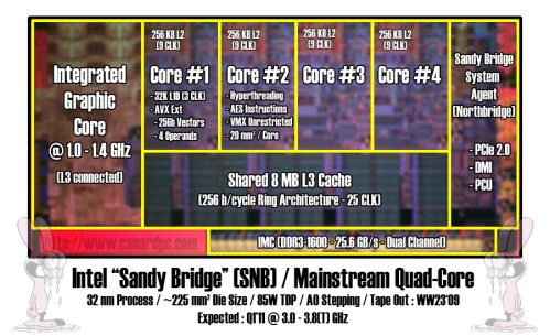
We were hoping that any kind of disclosures regarding Intel’s 32nm ‘Sandy Bridge’ architecture could wait until a year from now so that its upcoming 32nm Westmere predecessor would be enjoyed a bit longer. However, this is not the case as CanardPC has outspokenly revealed a die shot of the future architecture as well as its operating speeds.

The first and newest A0 silicon was taped out in week 23 of
this year, between June 1st and June 7th last month. The die pictured above
will be implemented as Intel’s mainstream 32nm quad-core models of Sandy
Bridge. These chips will feature 256KB L2 caches with clock speeds ranging from
2.8GHz to 3.4GHz, complete with Turbo Boost for additional performance as found
in the current Nehalem architecture.
In the first half of 2010, Intel plans to launch its first 32nm
chips known as Westmere to keep its current “tick tock” strategy rolling
along. Nehalem in Q4 2008 was a “tock” and a significant architectural leap
from its 45nm Penryn predecessor. Westmere will be a “tick” and a 32nm full
node die-shrink of Nehalem in H1 2010, followed by an architectural “tock”
rebound by Sandy Bridge in the first quarter of 2011. According to the latest
Intel roadmap, Sandy Bridge will then be replaced with a 22nm “tick” die-shrink
towards the end of 2011 rumored to be known as Ivy Bridge.
A key point of focus regarding these three upcoming microarchitectures
is that they will all include some sort of integrated graphics package, at
least in their mainstream model sets. Intel will start with 32nm Westmere by creating
a two-chip design with a 45nm IGP (GMA) and 32nm CPU in one
package. The architectural transition to Sandy Bridge will then integrate a
die-shrunk 32nm IGP directly into the CPU core itself for a single-chip
package, similar to AMD’s Fusion project codenamed
‘Swift’ that has been talked about for a while now. Finally, the entire
package will encounter another full node 22nm architectural shrink and Intel’s
CPU/GPU package will continue into the future.
Meanwhile, the graphics core in Sandy Bridge will run between
1GHz and 1.4GHz and will be connected to the shared 8MB L3 cache. The
integrated memory controller, or northbridge, is managing the L3 cache which
means that the IGP will benefit from L3 caching just as the CPU cores do. The
IMC in the new “tock” architecture is expected to run at a stock speed of DDR3
1600MHz, up from the stock 1066MHz found in Nehalem.
As for the high-end Sandy Bridge chips, there haven’t been
any disclosures as of yet but we are assuming they will be eight-core models
without IGPs (GMA) for the sake of the enthusiast crowd. There is also a
question of whether PCI-Express will shift from the 2.0 spec to 3.0 which has been
unanswered by Intel for quite some time, considering that its latest roadmaps
expect products implemented with it in 2010. All in all, it is expected that
mainstream Sandy Bridge chips will be placed with a new chipset on socket LGA
1156 in 2011, while the high-end fate is yet to be determined.

